KLA, leading provider of precision microstructure, surface profilers and surface measurement systems is a $9.7B company and has invested $4.6B in R&D in the last 4 years. With more than 72,300 instruments installed worldwide, KLA dominates the industry. ![]()
The KLA Instruments comprehensive portfolio of products, software, analysis, services and expertise is designed to help scientists, researchers and engineers address their toughest measurement challenges by generating reliable, precise data. Through use of these products and services, they are better able to deliver the breakthroughs that impact their respective fields.
Nano Technology Solutions is the exclusive distributor of KLA Instruments and supplies, installs, supports surface metrology products and accessories across Australia and New Zealand. Contact us to discuss your specific requirements and applications.
Stylus Profilers
Why choose a Stylus Profiler?
- An advantage of the stylus measurement technique is that it is a direct measurement, independent of material properties.
- Adjustable force and choice of stylus enable accurate measurements of a wide variety of structures and materials.
- These features enable quantification of feature topography to determine the amount of material added or removed, measurement of roughness, and stress caused by changes in the structure of the material.
- Stylus profilers have wide applications across many industries for monitoring production, development, and quality control processes. They are also well-suited for general use in universities, research labs, and institutes.
KLA Stylus Profilers
Since the launch of the Alpha-Step 100 stylus profilometer in 1977, KLA’s technical experts have continued to bring key innovations such as advanced topography sensors, ultra-flat scanning stages and fully automated measurement capability to market. KLA’s tools continue to evolve, providing repeatable and accurate measurements for your surface metrology requirements. Learn more about the rich history of innovation of KLA stylus profilers.

KLA’s range of stylus profilers deliver high-precision, 2D and 3D surface metrology, measuring step height, surface roughness, bow and stress with industry-leading stability and reliability for your R&D and production requirements. Visit the following pages for detailed information on our products and their applications:
- Complete product range and general features of KLA stylus profilers
- Alpha-Step D-series Stylus Profilers: ‘Development’-Series bench-top systems suitable for R&D and product development
- Tencor P-Series Stylus Profilers: ‘Production’-Series systems suitable for R&D, semiconductor and pilot-scale applications
- HRP-Series Automated High-Resolution Stylus profilers: suitable for high-throughput industrial-scale applications
KLA P-series Stylus Profilers have been chosen by leading Australian Universities, CSIRO and Defence Science & Technology Group. The unmatched performance of P-7 Stylus Profiler is achieved by revolutionary UltraLite® sensor which delivers ultra-high resolution of 0.01Å. The UltraLite® sensor incorporates an LVDC sensor technology with the lowest mass, lowest noise, and highest resolution of any sensor available today.
Nano Technology Solutions have KLA factory trained engineers on these metrology products and can guide you on the right configuration suitable to your research needs.
Optical Profilers
Why choose an Optical Profiler?
The demand for accurate characterisation of delicate samples and high aspect ratio geometries such as narrow gaps, deep trenches or deep holes arises in many technologies and industries. One of the more challenging measurements for a traditional optical profiler is the measurement of multi-dimensional, multi-material surfaces that provide varying levels of reflectivity. When a single sample contains both very low reflectivity surfaces and high reflectivity surfaces, measurement becomes a challenge as a much smaller amount of light reaches the optical sensor from a lower reflectivity surface than it does for a higher reflectivity surface. Similarly, very rough, or very sloped surfaces limit the amount of reflected light reaching the optical sensor making simultaneous measurement of these surfaces difficult.
KLA’s Zeta optical profilers are flexible and accurate tools for non-destructive and high-throughput surface topography measurements. They are powered by patented ZDot technology and Multi-Mode optics, enabling measurement of a variety of samples: transparent and opaque, low to high reflectance, smooth to rough texture, and step heights from nanometres to millimetres.

Zeta and Profilm Optical Profilers
KLA offers a wide range of instruments for different application requirements:
- The Zeta-20 Benchtop system is a non-contact, 3D microscope and surface topography measurement system, which is one of the best in the market for R&D and product development processes. It is a Multi-Mode optical profiler that integrates six different optical metrology technologies in one configurable and easy-to-use system.
- The Zeta-300 is a larger optical profiler suitable for Pilot-scale metrology requirements with an open configuration for handling much larger samples.
- The Zeta-388 is a fully-automated optical profiler with a larger, motorised wafer-handling configuration, suitable for production/fabrication facilities.
- The Zeta-Solar optical profiler is specifically designed for use in Solar Cell characterisation applications.
The newest generation of the Filmetrics ProFilm3D optical profiler is designed to specifically address the challenges where larger variations in surface topography and reflectivity require resolution of fine detail. They are cost-effective, easy-to-use systems suitable for measurements from polished optics to microfluidics channels, circuit boards, biological samples, biomedical devices, solar cells, and micro-machining.
Applications

- Photovoltaic Solar Cells
- Microfluidic Devices
- Semiconductor wafer analyses
- 3D and Flash Printing
- Metal Finishing / Micromachining / Tooling
- Optical micro-lens characterisation
- Patterned Sapphire Substrate
- Wafer Level Packaging
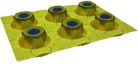
- VCSEL Devices
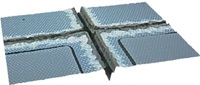
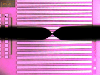
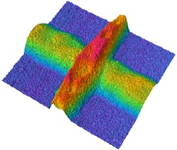
- Laser Dicing in LED characterisation

VCSEL Device 3D surface Profile using Zeta 20 
Laser Dicing analysis using Zeta 388 Optical Profiler - Biotechnology