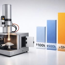
Common problems in Conductive AFM (Atomic Force Microscopy) include difficulty in managing high and low currents and avoiding unwanted side-effects such as the Joule, Bimetallic and local oxidation effects when using high currents. In order to produce accurate and reproducible measurements, constant tip replacements, re-setting up of the AFM, re-finding the area of interest are needed – all at the expense of time, money and effort.
Working of Conductive AFM
Working with Conductive AFM requires application of DC bias between the tip and the sample and the current flowing through the tip is measured. A Linear or logarithmic amplifier is used and the operator must select the range on the amplifier depending on the conductivity of the sample. Linear amplifiers generally cover a dynamic range of 3-4 orders of magnitude which is too limited to measure samples with both conductive and isolating domains. Logarithmic amplifiers have a dynamic range of 6-7 orders of magnitude however they are temperature dependant and slow (~0.1 line / sec) for measuring low currents.
Joule Effect
Imagine a sample with varying conductivity being scanned under Conductive AFM. When the tip reaches an area of high conductivity, the current flowing through the nanoscale tip causes self-heating of the tip due to Joule effect. This high heat can melt the thin conductive coating, break the conductive path and leave the tip unusable for Conductive AFM work.
Probe-induced Local Oxidation Effect
Another effect that may influence the conductive measurements is the so-called probe-induced local oxidation. This effect arises when there is a water layer adsorbed on the surface of the substrate. As the metallic tip is biased with respect to the sample, the presence of water in between creates a nano-electrochemical cell confined in the proximity of the tip apex. A local oxidation reaction then takes place. Sometimes this is highly noticeable as an oxide bump seen in the substrate. In other cases (depending on the bias, substrate, metallic coating etc.), it is noticed as a change in the current values. In the end this is an effect associated to current flow.
Bimetallic Effect
Another issue often overlooked is the bimetallic effect. The thermal expansion coefficient of the conductive coating is quite different to the cantilever material. As the tip scans over areas of varying conductivity, the current and thus, the temperature of the cantilever changes resulting in an additional extended force acting on the whole cantilever length (which can lead to quasi-static deflections of several tens or hundreds of nm). This additional force makes difficult to ensure a constant contact-area during the scanning as the feedback only acts on the tip-apex (i.e., a point-force). Maintaining a constant force (contact area) is crucial to obtain reproducible and reliable conductive measurements in AFM.
A study in recently published book by Mario Lanza explains these issues with supporting data (Chapter 12, Pacheco and Martinez. 2017). The study further describes a more effective conductive measuring concept, a module named ResiScope II from AFM manufacturer Concept Scientific Instruments, which overcomes these issues. This module allows to perform current/resistance measurements over 10 orders of magnitude (from fA to mA).

In the study, the ResiScope II module was used to scan well-defined conductive and non-conductive sample consisting of micron-sized graphene oxide domains over gold substrate. The high dynamic range of ResiScope II efficiently captured conductivity differences on the graphene oxide regions that were correlated with the thickness of the layer. This smart module works much faster (5 kHz) than the AFM tip moving from one pixel to another, enabling it to measure both highly conductive (gold) and insulating (graphene oxide) domains without transient effects or saturation in the gold areas. In addition, the ResiScope module can limit the actual current flowing through the tip and sample which minimises side effects of high currents as described above. The study shows a direct comparison between standard Conductive AFM and the ResiScope measurements on the same gold-graphene oxide surface. The results of the standard Conductive AFM current map showed typical features of conductive measurement on the sample with highly conductive domains. However, the conductivity was stable only in some areas. In other areas, the conductivity was lost. The conductivity was recovered again after several lines, but the current values were different. When using the ResiScope mode, the current map was stable during the entire scan.
This study demonstrates how the ResiScope can efficiently map both highly conductive and insulating domains without undesirable side-effects like probe-induced local oxidation, bimetallic effect or melting of the conductive coating by Joule effect.
ResiScope II can potentially transform the understanding of variable conductivity samples using Conductive AFM.
NanoTechnology Solutions is the exclusive distributor of this AFM in Australia and New Zealand.
Click here for more info on this AFM.
Update: There is now an extension of ResiScope II available which is tailored for conductive polymers and soft materials. It is called the Soft ResiScope.