QUANTAX EDS for TEM
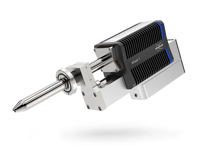
Bruker EDS for STEM, TEM and T-SEM: XFlash 7T slim-line detectors and ESPRIT software for nanometre and atomic-scale mapping.
Key features
- Microscopes
- Configured for each STEM, TEM or SEM (T-SEM): slim-line detector design optimised for the microscope's pole piece and EDS flange.
- Collection
- Maximum collection and take-off angles for fast, highly sensitive acquisition.
- Clean data
- Designed to avoid mechanical and electromagnetic interference, and to minimise specimen tilt, absorption, shadowing and system peaks.
- Atomic-scale mapping
- Drift correction for periodic structures (atoms, layers) and a fast-moving, stable detector stage.
- TEM quantification
- Cliff-Lorimer (theoretical and experimental factors) and Zeta-factor methods, with interpolation of missing Zeta-factors and absorption correction.
- In-situ experiments
- Time-resolved acquisition saves a stream of changing data, for example at elevated temperatures.
- Automation
- Scripting and API options for specific analysis jobs and batch processing; off-line analysis for student or laboratory networks.
Specifications
From Bruker's product page.
| Upper energy limit | 80 keV |
|---|---|
| Stable resolution | 1 Å |
| High-energy element lines | Above 40 keV, available for quantification |
| Quantification approaches | 3: theoretical and experimental Cliff-Lorimer factors, and Zeta-factors |
| Background models | 3: physical (bulk), physical (thin lamellae) and mathematical |
| Detector | XFlash 7T |
| Largest solid angle | > 1.1 sr |
|---|---|
| Analytical throughput | Up to 1,000 kcps (ISO 15632:2021) |
| Atomic database | More than 2,200 element lines |
| Uptime | SDD module exchange on site |
Resources
Webinars and videos
From the manufacturer's own channels.
-
XFlash 7 - The latest EDS Detector Series for Electron Microscopes Video · 9 June 2022 · Bruker
XFlash 7 - The latest EDS Detector Series for Electron Microscopes