 Built on 30 years of backscatter electron detector experience the microprocessor controlled Gen5 electronics offers unrivalled speed, sensitivity and low noise.
The Deben Gen5 amplifier system has four BSE input channels and a choice of one or three simultaneous video output channels.
Unlike standard OEM back scattered detectors our BSE system provides an unrivalled level of adjustment permitting highly optimised images to be acquired. Matched to the latest developments in our low kV silicon detector technology, diodes are mounted on a retractable arm or in some cases directly to the objective lens.
Features:

- Choice of 10mm, 18mm or 24mm four quadrant detector diodes
- Four input channels
- One output channel (optional three)
- AUX video input required on SEM for synchronised video display
- 8,000,000 to 1 amplification
- TV rate imaging with excellent quality
- Unique FIND feature
- Highly repeatable re-positioning
- Multiple parameters for optimisation
- PC control (compatible with Windows XP/7.0 Professional 32/64bit)
- RS232 or USB connectivity
- OEM versions available (including DLL library for software integration)
- UHV version available
Motorised insertion:
The motorised arm provides three positions; inserted, park (semi-retracted), as well as fully retracted. Alignment of the detector position is normally better than 20µm. Control is via software or keypad, motorisation is particularly useful when the detector is mounted in an inconvenient position such as to the rear of the column, or when used in a hazardous environment such as a ”hot cell”.
- Precision Detector Alignment, <20µm
- Three Positions
- Simple computer control
A scintillation type Cathodoluminescence detector providing monochromatic images, with a quickly removable tip it can be converted to a Back Scattered Electron (BSE) detector giving additional function for little extra cost.
Centaurus gives excellent images at low kV – ideal for those studying fragile and beam-sensitive samples. Changing from CL to BSE is easily achieved by swapping the mirrored tip to a phosphor coated tip. A suitable free chamber port and AUX video input are required on the SEM.
Cathodoluminescence (CL):
- Available for most conventional tungsten and FEG SEMs
- Excellent low kV performance
- High performance parabolic collection mirror
- High spatial resolution
- Operates in HV and LV mode
- Compositional monochromatic video output
- Dynamic range: 185-850nm (standard), optional wider range (400-1200nm)
Backscatter (BSE):
- Good atomic number resolution
- Dynamic range: 300-650nm
- High performance parabolic scintillator
System options:
Motorised insertion with Bellows sealing: The Motorised Centaurus Detector has all the functions of the manual model but with motorised insertion and welded bellows sealing. Its main application is for mounting in an inconvenient place, often behind the electron optical column. Its use is invaluable systems used in hazardous environments such as ”hot cells”.
Additional BSE or CL tips: Purchase a CL system with additional BSE tip.
Exchangeable PMTs: PMT tubes are user exchangeable to optimise collection wavelength.
A retractable PN diode semiconductor STEM detector configured with four Dark Field (DF) diodes wired as two pairs and a single Bright Field (BF) diode. The system may be operated in BF mode, DF mode or DF Phase Contrast mode along with mixing between segments, DF+BF for example.Twelve 3mm grids can be fitted to the standard STEM grid holder, allowing multiple specimen analysis. A retractable arm complete with Deben Gen5 electronics allows the STEM Detector to be used with any SEM with a free chamber port and AUX video input. The 12 position grid holder is airlock compatible and supplied complete with stage dovetail/sledge as required.
The STEM detector assembly uses a single Bright Field and 4 element Dark Field diode. Such is the performance of this design that it has proved equally successful fitted to both FEG and Tungsten SEMs. The STEM detector assembly inserts below the grid holder and has X,Y, Z position adjustment. Dark field diodes are configured so they can operate in full Dark Field or Dark Field Phase Contrast mode.
Deben Gen5 electronics is configured with four input channels and a single video output channel (optional two or three simultaneous video outputs).
The unrivalled scope of adjustability available to the operator then permits highly optimised images to be taken.
Features:
- Single bright field and four element dark field diode
- Imaging modes: Bright Field, Dark Field, Dark Field Phase Contrast or Mixed signal
- 8,000,000 to 1 amplification
- Unique image FIND feature
- Highly repeatable
- Multiple parameters for image optimisation
- One output channel (optional three)
- AUX video input required on SEM for synchronised video replay
- TV rate imaging with good quality
- PC control (compatible with Windows XP/7.0 Professional 32/64bit)RS232 or USB connectivity
- OEM versions available (including DLL library for software integration)
Motorised insertion:
The motorised arm provides three positions; inserted, park (semi-retracted), as well as fully retracted. Alignment of the detector positions is normally better than 20µm. Control is via software or optional keypad, motorisation is particularly useful when the detector is mounted in an inconvenient position such as to the rear of the column, or when used in a hazardous environment such as a ”hot cell”.
- Precision Detector Alignment, <20µm
- Three Positions
- Simple computer control
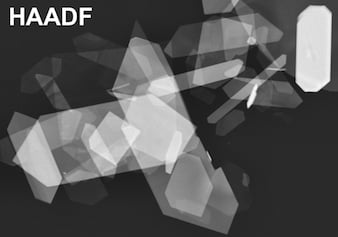
High Angle Annular Dark Field (HAADF) Scanning Transmission Electron Microscopy (STEM) is a very powerful technique to provide direct information on a local chemistry of nano-materials at atomic scale. Using the retrofit Deben Annular STEM, SEM users can acquire HAADF transmitted electron images for a fraction of the cost of a dedicated Transmission Electron Microscope (TEM) with HAADF detector fitted.
Twelve 3mm grids can be fitted to the STEM grid holder, allowing multiple specimen analysis. A retractable arm complete with Deben Gen5 electronics allows the STEM Detector to be used with any SEM with a suitable free chamber port and AUX video input. The 12 position grid holder is airlock compatible and is supplied complete with a stage dovetail/sledge as required.
Features:
- Low kV DF operation (1kV to 30kV)
- Bright field, LAADF, MAADF & HAADF detector segments
- Three simultaneous video outputs, eg. LAADF, MAADF & HAADF
- Resolution close to that of the SEM (in SE mode)
- 12 position 3.05mm grid holder
- High speed TV rate imaging
- Motorised insertion & retraction
- PC controlled with USB interface
Motorised insertion:
The motorised arm provides three positions; inserted, park (semi-retracted), as well as fully retracted. Alignment of the detector positions is normally better than 20µm. Control is via software or keypad, motorisation is particularly useful when the detector is mounted in an inconvenient position such as to the rear of the column, or when used in a hazardous environment such as a ”hot cell”.
- Precision Detector Alignment, <20µm
- Three Positions
- Simple computer control


 The Specimen Current-EBIC Amplifier is designed to operate with the small currents absorbed by the sample in the SEM. The system gives accurate absorbed current measurements but will also provide images over a wide range of probe currents.
When a high-energy electron penetrates a crystalline semiconductor, most of its kinetic energy is absorbed by ionization of the silicon atoms as silicon valence electrons are ejected from their orbits. Each ionization creates a free electron and the empty valence site leaves the atom electrically unbalanced with a net positive charge. This net positive charge called a hole appears to migrate from atom to atom under the influence of an external field creating the illusion of a flow of positive charge. At the interface of P-doped and N-doped regions.
 There is a narrow zone void of mobile charge carriers due to the electric field (Fermi Potential) created by the redistribution of electrons and holes at the junction. If the electrons and holes created by the impinging electrons can enter this Depletion Zone, then they, too will be swept aside by the Fermi Potential:this movement of charge carriers manifests itself as a current in an external circuit. In Silicon the average electron hole pair requires about 3.6eV of energy so that the external current, which is proportional to the number of carriers entering the Depletion Zone, may well be two to four orders of magnitude greater than the primary beam current depending on the primary beam energy and the percentage of the pairs that can be absorbed into the Depletion Zone. This phenomenon is known as Electron Beam Induced Current or EBIC. This same effect can be induced by photon bombardment and is the basis for the operation of photodiodes and solar cells.
Modern planar semiconductor devices, because of their uniquely two- dimensional structure, lend themselves readily to both qualitative and quantitative investigation by the EBIC technique in the Scanning Electron Microscope and also in the Laser Scanning Microscope (OBIC).