NanoTechnology Solutions provides advanced instrumentation to Australia’s leading research and industrial facilities.
The advancement of materials science relies heavily on Electron Backscatter Diffraction (EBSD) to provide crystallographic data at the nanoscale. However, the efficacy of EBSD is fundamentally limited by the quality of the specimen surface. Recognising a significant market gap where researchers struggled with inconsistent indexing and surface artifacts, NanoTechnology Solutions introduced the COXEM IP-10k argon ion milling system to the Australian market. This instrument addresses the critical “damaged layer” problem, enabling researchers to unlock the full potential of high-speed detectors like the Bruker eWARP and high-precision Bruker ED-XS (EDS) systems.
The Physics of the ‘Damaged Layer’ in Mechanical Polishing
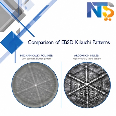
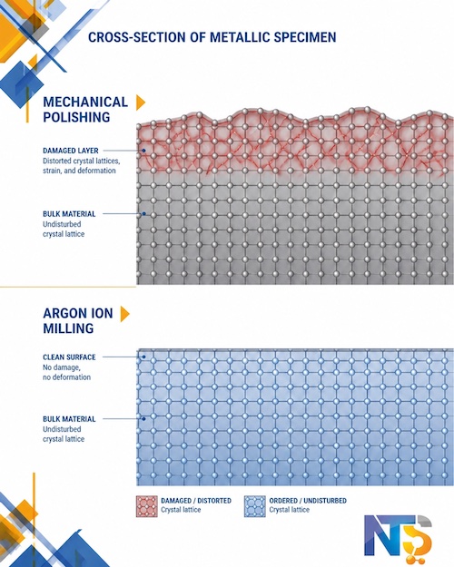
The primary challenge in EBSD specimen preparation is that the diffracted electrons originate from the top 10–50 nm of the sample surface. Traditional mechanical polishing, while effective for general metallography, inherently introduces physical deformation at the atomic level.
- Plastic Deformation: Abrasive particles create a work-hardened, plastically deformed layer that disrupts the crystal lattice.
- Residual Strain: Mechanical force leaves behind latent strain that degrades the quality of Kikuchi patterns.
- Contamination: Polishing suspensions can embed silica or alumina particles into softer phases, creating false features.
- Surface Relief: Differential polishing rates between hard and soft phases in multiphase materials lead to topography that causes shadowing in the SEM.
When these defects are present, the EBSD detector receives “blurred” or low-contrast signals, significantly reducing the Indexing Success Rate (ISR).
The Solution: Argon Ion Milling with the COXEM IP-10k
The COXEM IP-10k employs a broad-beam argon ion source to remove material at the atomic level. Unlike mechanical polishing, Argon Ion Milling is a non-contact process that effectively strips away the damaged surface layer to reveal the native, pristine crystal structure beneath.
Technical Capabilities of the COXEM Ip-10k:
- High-Speed Milling: Capable of material removal at rates exceeding 100 µm/hour for certain materials.
- Voltage Range: Adjustable from 1 kV to 10 kV, allowing for aggressive material removal or gentle final polishing at low energies.
- Cooling Systems: Integrated cooling prevents thermal damage to heat-sensitive specimens like polymers or low-melting-point alloys.
- Versatility: This system supports both Cross-Section Polishing (using a metal mask for precise edges) and Flat Milling for large-area EBSD maps.
By using the COXEM IP-10k, researchers ensure that the top 10 nm of the sample is strain-free and perfectly flat, providing the high-contrast Kikuchi patterns required for advanced characterisation.
Synergising with Bruker eWARP and ED-XS Technology
For laboratories utilising Bruker microscopy accessories, the integration of an ion-milled surface is not merely beneficial: it is essential for peak performance.
Enhanced EBSD Indexing with Bruker eWARP
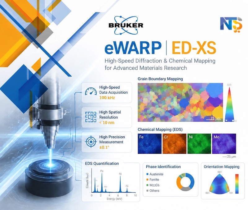
The Bruker eWARP system represents the state-of-the-art in high-speed EBSD processing, capable of correcting for drift and distortion in real-time. However, even the most advanced algorithms cannot compensate for a lack of signal.
- Higher Pattern Quality Index (PQI): Ion milling ensures that the eWARP software can identify band edges with higher precision.
- Distortion Correction: A flat, ion-milled surface provides stable imaging, allowing eWARP to apply accurate geometric warping corrections without being misled by surface topography.
- High-Speed Mapping: With the COXEM IP-10k‘s preparation, users can push Bruker detectors to their maximum acquisition speeds while maintaining ISR above 99%.
Precise Chemical Mapping with Bruker ED-XS
When performing simultaneous EBSD and EDS (Energy Dispersive Spectroscopy), surface cleanliness is paramount. The Bruker ED-XS detector benefits from:
- Removal of Oxides: The argon beam removes surface oxidation that can skew light-element quantification.
- Zero Residue: Unlike chemical etching, ion milling leaves no chemical residue, ensuring the EDS spectra reflect the true bulk composition.
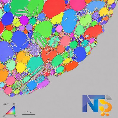
- Spatial Correlation: The lack of relief ensures that chemical boundaries in EDS maps align perfectly with crystallographic boundaries in EBSD maps.
Catalog of Applications and Performance Metrics
The combination of the COXEM IP-10k and Bruker analytical tools is particularly effective for several challenging material classes:
1. Martensitic Steels and Nickel-Superalloys
- Problem: High hardness and complex phases make mechanical polishing difficult.
- Ion Milling Benefit: Reveals fine needle-like martensite structures without smearing.
- Metric: Achieves indexing in regions previously considered “un-indexable” due to high dislocation density.
2. Layered Semiconductor Devices
- Problem: Mechanical rounding at interfaces of dissimilar materials (e.g., Si vs. Au).
- Ion Milling Benefit: The metal mask on the IP-10k produces a 90-degree cross-section with zero edge rounding.
- Metric: Interface resolution at the sub-micrometre scale.
3. Geological and Mineralogical Specimens
- Problem: High porosity and varying mineral hardness.
- Ion Milling Benefit: Prevents “plucking” of grains and produces a uniform surface for metrology and 3D surface profiling.
Conclusion: Elevating Research Workflows
The path to high-resolution crystallographic data begins long before the electron beam is activated. By incorporating the COXEM IP-10k into the workflow, researchers are able to remove the variables introduced by manual preparation. When paired with the high-speed processing power of Bruker eWARP and the analytical accuracy of Bruker ED-XS, the result is a robust, reproducible, and highly efficient microscopy platform.
For more information on optimising your sample preparation, explore our range of ion beam polishers or contact our technical team to discuss plasma cleaning and vibration isolation solutions for your SEM suite.