COXEM is a leading manufacturer of Scanning Electron Microscopes (SEM) utilising technology developed with KRISS, the Korean Research Institute for Science and Standards. With its latest products, it is expanding the capabilities of entry to mid-level SEM analysis at affordable costs. With on-going investments in research and product development, COXEM Co., Ltd. is the fastest growing supplier of SEMs and peripheral instruments like Ion Beam Polishers and Sputter Coaters in the scientific market.
NanoTechnology Solutions is the exclusive distributor of COXEM’s instruments in Australia and New Zealand, offering installation, service and technical support for a range of applications. Contact us to discuss your Electron Microscopy needs.

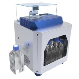
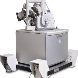
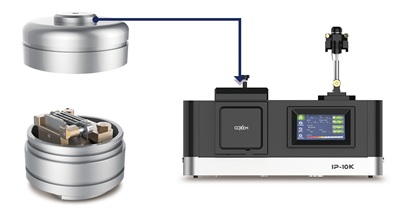
COXEM IP-10K
The IP-10K is COXEM’s upgraded Ion Beam Polisher. It is an advanced sample preparation tool that can be used to polish or etch the surface of samples for subsequent observation in Desktop and Portable SEMs. It is equipped with various modules including flat-milling, cooling stage, and the air-protection module, to meet precise, high-quality sample preparation needs for applications such as WDS, SEM, EBSD and EDS analyses.
Mechanism of Ion Beam Polishing
When a voltage is applied to the ion gun and argon gas is injected, plasma is generated and an argon ion beam is directed at the sample by an acceleration voltage to begin the etching process. If the sample is located behind a metal mask and the ion beam is directed at the metal mask and sample, the shielding effect of the metal mask minimises beam damage to obtain clean cross-sectional etching results. Since the polishing speed, area, and depth vary depending on the angle of incidence at which the ion beam hits the sample surface, uniform surface polishing is induced by rotating and adjusting the angle of the sample.

Cross-sectional ion beam polishing has the following advantages:
- Unlike mechanical polishing where it is difficult to check the exact state of the cross section due to physical damage and contamination, with ion beam polishing, you can observe the micro-surface structure of the sample without structural damage and contamination or complicated chemical processes.
- Compared to focused ion beam (FIB), you can achieve excellent time and cost savings by etching a much wider cross section of a single side of the same sample in a shorter time.
It is evident how much cleaner the cross-section surface appears after ion beam polishing compared to images of fractured or mechanically polished samples.

Why IP-10K is ideal for SEM applications
The IP-10K offers unparalleled capabilities for the precision milling of materials at the microscale levels, providing exceptional cleanliness and accuracy:
- A fast milling speed of 1,000um/h (Si, 8kV)
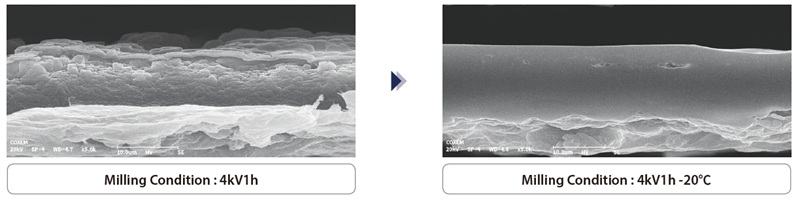
- Minimises thermal damage with a Peltier-type cooling stage: capable of cooling down to -20ºC for working with heat-vulnerable samples.
- Air-protection module compatible with SEM: This option allows milling and observation of samples prone to degradation upon exposure to the air.
- Flat-milling function provided for planar etching: When a sample is mounted in the dedicated holder and the flat milling function is used, several square millimetres of area are etched by the ion beam based on the rotation centre axis.
- Ion Beam On/Off timer: A feature designed to minimise heat damage for obtaining accurate cross-sectional conditions when etching heat-sensitive samples such as polymers and paper.
- Noise, vibration, oil-free diaphragm pump with a fast pump/vent time.
- Higher front mask usability: for cleaner, more controlled polishing and etching
- Recipe Mode: Ability to save/load etching recipes that are frequently used. In addition, a step-by-step mode is also available to automatically execute serial recipes.
- Built-in digital microscope and chamber camera: for fast sample alignment and real-time observation of etching status.
- Convenient operation: intuitive GUI and easy touch screen and sample loading using smart sample holder.
Applications of Ion Beam Polishing
Apart from being widely used in applications such as semiconductor processing, solar cell characterisation, powder analysis, etc., it is a useful step in the following analyses:
- EPMA (Electron Probe Microanalysis): since the system provides ion milling of large areas of the sample, from tens of um to several mm, it is useful for removing the oxide layer and foreign substances in the sample cross section. This enhances the quality and quantitative accuracy of EPMA component analysis.
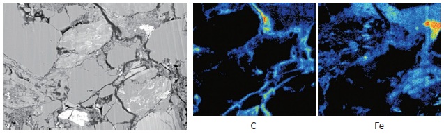
- EDS (Energy Dispersive X-ray Spectroscopy): By etching a sample with an ion beam to minimise damage to the cross-sectional structure and analysing the components with EDS, the exact distribution of surface components can be observed without structural distortion of the sample.
- EBSD (Electron Backscatter Diffraction): In the crystallography of metallic materials, precise surface pre-treatment is a very important factor for accurate grain and grain boundary analysis of metal samples. Ion beam milling is an ideal method to prepare samples prior to studying the mechanical and electrical properties of the sample through EBSD analysis.
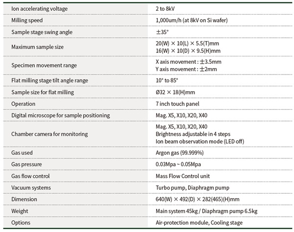
Specifications