![]() KLA Instruments’ Tencor P-series Stylus Profilers deliver high-precision 2D and 3D surface metrology, measuring step height, surface roughness, bow, stress and other challenging analyses by generating reliable, precise data with industry-leading stability and reliability. They have been chosen by leading Australian Universities, CSIRO, and Defence Science & Technology Group.
KLA Instruments’ Tencor P-series Stylus Profilers deliver high-precision 2D and 3D surface metrology, measuring step height, surface roughness, bow, stress and other challenging analyses by generating reliable, precise data with industry-leading stability and reliability. They have been chosen by leading Australian Universities, CSIRO, and Defence Science & Technology Group.
Nano Technology Solutions is the exclusive distributor of KLA Instruments and supplies, installs, supports surface metrology products and accessories across Australia and New Zealand. We have KLA factory-trained engineers on these metrology products and can guide you on the right configuration suitable for your research needs.
Contact us to discuss your specific requirements and applications.
Tencor P-Series Stylus Profilers are ‘Production series’ instruments ideal for the demands of greater performance at Semiconductor fabs and industrial-scale applications. They utilise advanced LVDC (Linear Variable Differential Capacitive) sensor technology which has the following outstanding benefits:
- It can measure features up to 1mm in height or depth while enabling high Z resolution capability that delivers 0.001Å z resolution in the lowest vertical range (1μm step) and 0.60Å z resolution in the highest vertical range (1000μm step).
- A fast linear response to accurately track changes in surface topography, enabling fast measurement speeds for small and large step heights.
- Low hysteresis and low friction enable precise, stable, high resolution measurements across the full vertical range over long periods of time.
- The design uses an electronic force coil, enabling closed loop software control, which means the force is adjusted during scan to ensure a constant force is applied on the sample surface. This makes P-series instruments ideal for measurements with strict force requirements.
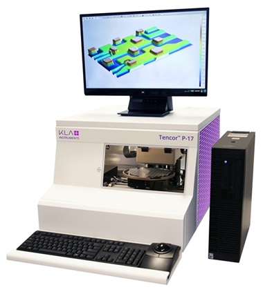
Tencor P-17
The Tencor P-17 is the eighth generation of the P-series stylus profilers, building on over 40 years of profilometry expertise. The system offers a programmable scan stage, low noise, and sub-Angstrom electronic resolution throughout the vertical range, enabling high-resolution scans across the entire sample surface.
The P-17 system benefits include a 200 mm scan stage for measurement of the entire substrate without the need to stitch. An UltraLite® sensor assembly combines a large, linear vertical range with constant force control to measure a wide variety of materials and topographies. The system includes a 200 mm scan stage. Top and side view optics enable easy site teaching, pattern recognition, and visualisation of the stylus during a measurement. The system can be configured to handle large sample wafers (300 mm wafers), or with a 240 x 240 mm chuck.
The P-17 combines automation with high reliability for addressing production applications where a wafer handler is not required. These applications include step height, roughness, and stress metrology for AlTiC, GaAs, Si, SiC, and sapphire wafers for use in semiconductors, power devices, wireless, LED, and data storage.
Tencor P-7

The P-7 stylus profiler builds on the success of the market-leading P-17 benchtop stylus profiling system and is a more compact system with a 150mm scan stage having all the same performance features as the P-17. The unmatched performance of P-7 Stylus Profiler is achieved by revolutionary UltraLite® sensor which delivers ultra-high resolution of 0.001Å. The UltraLite® sensor is an LVDC sensor with the lowest mass, lowest noise, and highest resolution of any sensor available today. It is the only sensor technology with constant force control over the entire vertical range. For measurements that have strict requirements of force, the P-7 is the most popular stylus profiler, especially in the semiconductor industry for lab-scale R&D and product development. Applications include measurements of step height, roughness, and stress metrology for AlTiC, GaAs, Si, SiC, and sapphire wafers for use in semiconductors, power devices, wireless, LED, and data storage.
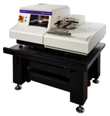
Tencor P-170
The Tencor P-170 system is a cassette-to-cassette profiler featuring the industry-leading benchtop system measurement performance of the P-17 stylus profiler and the HRP-260 system’s production-proven handler. It is a multi-purpose tool designed for production environments, including support for host control via SECS/GEM. Recipe setup on the P-170 system is fast and easy with point-and-click stage controls, dual-view optics and high-resolution digital cameras.
Fully automated measurements are achieved with automated wafer handling, pattern recognition, sequencing, and feature detection to place the cursors relative to the feature of interest. The advanced geometric pattern recognition algorithms and calibrations for X-Y and Z matching enhance recipe transportability between systems, satisfying a key requirement for 24×7 production environments. Wafer handler automatically loads and aligns 75mm-200mm opaque and transparent samples.
Measurement Capabilities
The P-Series profilers can be used to measure:
- 2D and 3D step heights from nanometres to 1mm, depending on the sensor assembly’s dynamic range. Quantify the material deposited or removed during etch, sputter, deposition, spin coating, CMP, and other processes.
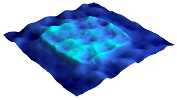
- 2D and 3D texture while quantifying and distinguishing the sample’s roughness and waviness components using software filters.
- 2D and 3D shape or wafer bow resulting from layer stress mismatch during the device fabrication process. Quantify the height and radius of curved structures, such as a lens.
- 2D and 3D stress metrology for AlTiC, GaAs, Si, SiC, and sapphire wafers. 2D stress mode uses a single scan across the sample diameter whereas 3D stress mode rotates the theta stage between 2D scans to measure the full sample surface.
- Topography of defects such as the depth of a scratch. Use KLARF defect inspection tools to automatically navigate to a specific defect for 2D or 3D measurement using the Defect Review application.
P-Series stylus profilers are highly versatile high-precision instruments used in a wide range of industries for production or R&D, including:
- LED and Power Devices: Measurement of step heights for patterning processes, including MESA step height, ITO step height, and contact depth as well as substrate roll off, bow, epitaxial roughness, and epitaxial thin-film stress that can lead to cracks and defects.
- Data Storage: Monitoring hard disk surface roughness, quantify hard disk roll-off (including chamfer angle and depth), thin film head bar roughness, and thin film head pole tip recession. Measurements of plating thickness, coil heights, and CMP planarity on wafers with low force to avoid scratching.
- SIMS (Secondary Ion Mass Spectrometry): Measurement of crater depth and roughness of the bottom surface with high precision to determine ion concentration as a function of crater depth and process uniformity.
- Textile: Measurement of textile security features or roughness correlating to absorbency.
- Biomedical: Measurements of catheter surface texture, medical stent reservoir depth, and the topography of metal cardiac implants.
- Electronics: Measurements of touch screen topography or thin film step heights on glass screens.
- MEMS and Optical Electronics: Measurements of step height, radius of curvature, and 3D topography for macro and micro lenses. Measure etch depth and surface roughness for waveguides and dense wavelength division multiplexing (DWDM) structures.
- 5G Applications (P-170): Measurements of topography and step height post-etch, pre-CMP, and post-CMP for a wide range of devices. Using the production features of the P-170 profiler, automatically measure multiple sites on the wafer for increased quality control at critical layers and improved device reliability.
For information on the Hardware and Software features of Tencor P-Series Profilers, click here.