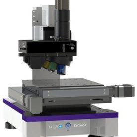
![]() KLA Instruments’ Alpha-Step D-Series, Tencor P-series, and HRP-Series Stylus Profilers deliver high-precision 2D and 3D surface metrology, measuring step height, surface roughness, bow, stress and other challenging analyses by generating reliable, precise data with their innovations in sensor technology.
KLA Instruments’ Alpha-Step D-Series, Tencor P-series, and HRP-Series Stylus Profilers deliver high-precision 2D and 3D surface metrology, measuring step height, surface roughness, bow, stress and other challenging analyses by generating reliable, precise data with their innovations in sensor technology.
Since the launch of the Alpha-Step 100 stylus profilometer in 1977, KLA’s technical experts have continued to bring key innovations such as advanced topography sensors, ultra-flat scanning stages and fully automated measurement capability to market. KLA’s tools continue to evolve, providing repeatable and accurate measurements for your surface metrology requirements. Learn more about the rich history of innovation of KLA stylus profilers.
Nano Technology Solutions is the exclusive distributor of KLA Instruments and supplies, installs, supports surface metrology products and accessories across Australia and New Zealand. We have KLA factory-trained engineers on these metrology products and can guide you on the right configuration suitable for your research needs.
Contact us to discuss your specific requirements and applications.
Stylus Profiler Sensor Design

The advantage of a stylus profiler is that it is a direct technique that is not influenced by the properties of the surface. The sensing system has four main components:
- Topography Sensor: The topography sensor is used to trace the surface of the sample being measured.
- Stylus: The stylus is the measuring probe attached to the topography sensor. KLA styli are manufactured from diamond and come in a variety of sizes to support various applications.
- Pivot: The pivot translates the change in motion of the stylus to the topography sensor. Low mass, frictionless pivots are used for accurate characterisation.
- Force Compensation: The force compensation mechanism is used to adjust the force that will be applied to the sample surface. This force can be applied open or closed loop. Open loop applies a constant force at the pivot, resulting in a variable force on the sample surface as the stylus follows the surface topography. Closed loop applies a constant force on the sample surface by adjusting the force applied to the pivot using a feedback loop from the topography sensor as the stylus tracks the surface topography.
The method to make these measurements has continuously improved, and one critical area of advancement is the topography sensor. There are three major sensor designs in use today – LVDT, Optical Lever, and LVDC.
The Linear Variable Differential Transducer (LVDT) sensor technology was first developed in the 1930s and it is the oldest design used for stylus profilometry, historically used in many different sensing applications and popular instruments like Dektak Stylus Profilers. The following drawbacks of LVDT make it unsuitable for high precision applications:
- Poor Z resolution
- The sensor module is heavy and the force applied is difficult to control and maintain.
- Limited range of applied force, with the lower limit capable of causing stylus damage and scratches on sensitive samples.
- The motion of the arm within the coil will heat and cool as a function of usage over time, reducing measurement stability.
Almost 20 years ago, KLA stopped using LVDT sensors even on its entry level stylus profilers. Currently the Optical Lever and LVDC technologies are used in the Development and Production Series products, respectively, for their individual merits. With over 40 years of success in stylus profilometry, KLA’s Profilers have the necessary range of capabilities to address the surface metrology challenges of both R&D and production environments.

Optical Lever Technology
The Optical Lever sensor technology was developed for AFMs in the 1980s and later adapted to stylus profilometry in 2001 with the release of the XP-Series stylus profilers. The sensor system has the following design:
- The Optical Lever sensor uses a laser beam which is reflected off the top surface of the pivot assembly.
- The reflected beam is then projected on a photodetector.
- For the Alpha-Step, the beam is split into two components: one side is projected onto a dual cell photodetector while the other side is projected onto a single cell photodetector.
- The deflection of the laser beam is converted to a topography signal to create the surface profile.

The Alpha-Step D-Series products are ‘Development series’ instruments widely used in R&D facilities. They utilise the Optical Lever sensor technology which provides the following benefits:
- The beam-splitting design enables high Z resolution measurements of smaller steps on the first detector and measurement of larger steps on the second detector.
- They can measure features up to 1.2mm in height or depth. These high resolution measurements deliver 0.38Å z resolution in the lowest vertical range.
- The low mass of the entire assembly enables low force measurements.
- The sensor has a fast response for tracking changes in the surface topography, enabling fast measurement speeds.
- The design uses an electronic force compensation circuit that enables software control of the applied force which is open loop and ranges between 0.03mg and 15mg.

LVDC Technology
The Linear Variable Differential Capacitor (LVDC) sensor design technology was developed in the 1990s by Tencor Instruments to solve the limitations of LVDT sensor technology. When it was patented, the LVDC sensor had an order of magnitude higher performance than the LVDT, which has improved even further over the years, as demonstrated by the very high Z resolution discussed below. It works based on the following principles:
- The LVDC sensor tracks the surface topography using a change in capacitance. This change results from the motion of a thin metal sensor vane moving between two capacitor plates.
- The position of the sensor vane changes as the stylus tracks the surface, resulting in changes in the capacitance, which is then converted to a topography signal.
The advantages of the LVDC design are its low mass and linear motion of the vane, resulting in minimal hysteresis and friction. The design enables precise, stable, high resolution measurements across the full vertical range.
Tencor P-Series Stylus Profilers include the P-7, P-17, P-17 OF, and P-170 profilers. They are ‘Production series’ tools that deliver the demands of greater performance at semiconductor fabs and multiple industrial-scale applications. They all utilise LVDC sensor technology. The HRP-Series automated High-Res profilers also use the LVDC technology. They have the following capabilities:
- The LVDC design can measure features up to 1mm in height or depth. The highly sensitive capacitive plate technology enables high resolution capability that delivers 0.001Å z resolution in the lowest vertical range (1μm step) and 0.60Å z resolution in the highest vertical range (1000μm step).
- The design uses an electronic force coil, enabling closed loop software control of the applied force. This closed loop design enables a constant force on the sample surface between 0.03–50 mg.
- The sensor design and control enable measurement of soft surfaces with large step heights, such as photoresist etch depth.
- LVDC sensor technology has a fast linear response to accurately track changes in surface topography, enabling fast measurement speeds for small and large step heights.
- Low hysteresis and low friction enable repeatable measurement results that are stable over long periods of time.
KLA P-series Stylus Profilers have been chosen by leading Australian Universities, CSIRO and Defence Science & Technology Group. The unmatched performance of P-7 Stylus Profiler is achieved by revolutionary UltraLite® sensor which delivers ultra-high resolution of 0.001Å. The UltraLite® sensor is an LVDC sensor with the lowest mass, lowest noise, and highest resolution of any sensor available today. It is the only sensor technology with constant force control over the entire vertical range, making it suitable for measurements that have strict requirements of force. The large optical flat stage, decoupled lead screws and special stage driving system deliver the most accurate single scans of 156mm length (6″ wafers) without stitching.