Research laboratories across Australia, Europe, and North America face a recurring challenge: selecting the appropriate surface characterisation technology for nanoscale measurements. The decision between an Atomic Force Microscope (AFM), Scanning Electron Microscope (SEM), and Optical Profiler directly impacts data quality, experimental throughput, and research outcomes.
This framework provides the technical criteria for making that selection based on resolution requirements, sample characteristics, and operational constraints.
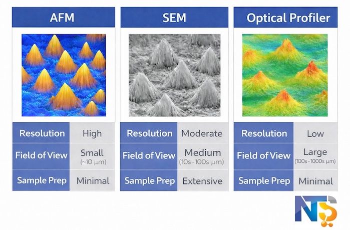
Understanding the Core Technologies
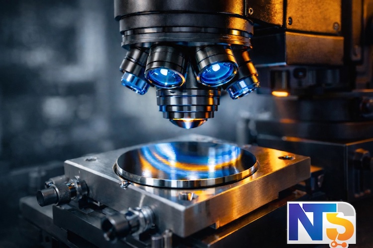
Atomic Force Microscope (AFM)
The AFM operates through direct mechanical probing of surface topography. A sharp tip mounted on a flexible cantilever scans across the sample surface whilst maintaining constant force or constant height. Deflection of the cantilever generates a three-dimensional surface map with sub-nanometre vertical resolution (instrument- and mode-dependent, and subject to calibration and noise floor).
Key specifications (typical, system- and configuration-dependent) include:
- Vertical resolution: ~0.1 nm (application-dependent)
- Lateral resolution: ~1–10 nm (often limited by tip radius and tip–sample convolution)
- Operating environments: vacuum, ambient air, controlled atmosphere, or liquid (model-dependent)
- Scan speeds: typically ~0.5–2 lines per second (depending on scan size, feedback settings, and SNR)
The technique provides 3D surface mapping without requiring conductive coatings or vacuum conditions for many sample types. AFM can also quantify nanomechanical properties including stiffness, adhesion, and friction via force spectroscopy and related modes (results depend on probe selection, modelling assumptions, and calibration).
Scanning Electron Microscope (SEM)
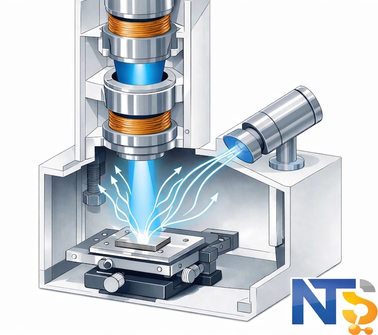
The SEM generates images by rastering a focused electron beam across the sample surface. Secondary electrons, backscattered electrons, and characteristic X-rays produced by beam–sample interactions provide contrast based on topography, atomic number, and elemental composition.
Performance characteristics (typical, system- and operating-condition-dependent) include:
- Lateral resolution: ~1.5–5 nm for modern field emission systems (dependent on kV, working distance, probe current, and sample)
- Imaging speed: real-time viewing to video-rate navigation (dependent on scan parameters and SNR)
- Field of view: millimetres to micrometres (dependent on working distance and magnification)
- Operating environment: high vacuum (often ~10⁻⁴ to 10⁻⁶ Pa; instrument-dependent)
SEM imaging supports rapid characterisation of large areas. The depth of field typically exceeds optical microscopy, enabling tilted samples and three-dimensional structures to remain in focus across a wider z-range. Height information is generally inferred from contrast, shadowing, and stereometric methods rather than direct, traceable height metrology without dedicated approaches.
Non-conductive samples often require charge mitigation (e.g., metal or carbon coating, low-kV imaging, variable-pressure operation): selection depends on feature size and analysis objectives. Where coatings are used, added thickness is commonly in the nanometre-to-tens-of-nanometre range and can obscure the original surface at the smallest length scales.
Optical Profiler
Optical profilometry measures surface topography through interferometry or focus variation techniques. White light or laser illumination reflects from the sample surface, and the interference pattern or focus position determines height at each point.
Technical specifications (typical, technique- and surface-dependent) include:
- Vertical resolution: ~0.1–1 nm (interferometric methods under suitable conditions; dependent on surface reflectivity, vibration, and algorithm)
- Lateral resolution: ~0.3–1 µm (diffraction-limited; dependent on objective NA, wavelength, and sampling)
- Measurement speed: complete area maps in seconds (dependent on area, sampling, and method)
- Operating environment: ambient air (common), with enclosures/isolated set-ups used where required
The technique requires no sample preparation for many surfaces and is non-contact, which reduces the risk of mechanically induced surface modification. For roughness characterisation across millimetre-scale areas, optical profilometry often provides higher throughput than point-by-point scanning methods, subject to surface optical properties and slope limitations.
The Selection Framework
Resolution Requirements
Vertical resolution determines the smallest height difference detectable (in practice: noise floor, bandwidth, calibration, and environmental stability). AFM can achieve ~0.1 nm vertical resolution under appropriate conditions. Optical profilers can achieve ~0.1–1 nm vertical resolution in interferometric modes on suitable reflective surfaces, with performance dependent on vibration, reflectivity, and algorithm selection.
Lateral resolution defines the smallest horizontal features resolved (often limited by probe geometry in AFM, beam interaction volume and landing energy in SEM, and diffraction in optical profilometry). AFM can achieve atomic-scale lateral resolution on selected crystalline surfaces under specialised conditions; for routine measurements, lateral resolution is commonly limited by tip radius (~1–10 nm effective). SEM field-emission systems commonly specify ~1.5–5 nm resolution under stated operating conditions. Optical profilers are diffraction-limited to approximately ~0.3–1 µm, which suits microstructures and surface texture but not nanoparticles or molecular-scale features.
Sample Considerations
Conductive samples work well in SEM without coating. Non-conductive materials require metal deposition for SEM imaging, which adds thickness and can obscure fine features. AFM and optical profilers measure non-conductive samples directly.
Delicate samples can be affected by AFM tip–sample interaction forces (often in the ~1–100 nN range depending on mode and setpoint). Optical profilers are non-contact. SEM electron beam exposure can induce charging, heating, or radiolysis in beam-sensitive polymers or biological specimens depending on dose and accelerating voltage.
Sample size influences technique selection. AFM typically accommodates samples up to 150 mm diameter but scans only micrometres at high resolution. SEM chambers accept samples from millimetres to 300 mm diameter with complete imaging. Optical profilers measure areas from micrometres to centimetres in single captures.
Environmental Constraints
AFM operates in multiple environments: ultra-high vacuum for surface science, ambient air for routine measurements, controlled atmosphere for reactive samples, and liquid for biological specimens (system- and accessory-dependent). This versatility supports electrochemistry, biomolecular imaging, and corrosion studies.
SEM typically requires high vacuum for electron optics and beam propagation (instrument-dependent). Environmental/variable-pressure SEM variants allow higher chamber pressures with corresponding trade-offs in achievable resolution and signal collection. Hydrated, volatile, or outgassing samples generally require preparation strategies appropriate to the microscope configuration and measurement objective.
Optical profilers typically operate in ambient air with minimal sample preparation. Enclosures, vibration isolation, and environmental control can be used where required by the noise floor and measurement uncertainty. Liquid immersion is generally not a standard operating mode for most optical profilometry configurations.
Decision Matrix
Choose AFM When:
- Atomic-scale resolution is mandatory (crystallography, molecular assembly, semiconductor defects)
- True 3D topography with quantitative height measurement is required
- Nanomechanical properties (stiffness, adhesion, friction) supplement topography
- Samples cannot tolerate vacuum or metal coating (polymers, gels, biomaterials)
- Liquid environment measurements are necessary (electrochemistry, biological processes)
- Nanoparticle dimensions below ~15 nm require metrology approaches with appropriate lateral resolution and traceable calibration (tip radius and deconvolution considerations apply)
Choose SEM When:
- Large area imaging at high magnification is needed (millimetre fields of view)
- High throughput characterisation of multiple samples is required
- Elemental composition analysis accompanies imaging (with EDS/WDS)
- Rapid screening precedes detailed measurements by other techniques
- Samples are conductive or easily coated without feature obscuration
- Internal structure visualisation requires cross-sectioning
Plasma cleaning before SEM imaging removes organic contamination that degrades image quality and detector performance. This preparation step enhances resolution for sensitive applications.
Choose Optical Profiler When:
- Rapid roughness measurements over large areas are sufficient
- Sub-micrometre resolution meets application requirements
- Non-contact, non-destructive measurement is mandatory
- Sample throughput exceeds AFM scanning speed capabilities
- Engineering surfaces require quality control rather than atomic detail
- Real-time process monitoring demands continuous measurement
Complementary Usage in Modern Laboratories
Advanced characterisation often requires multiple techniques applied to the same sample. A typical workflow combines:
- Optical profiler for rapid area mapping and feature location
- SEM for detailed morphology and elemental analysis of selected regions
- AFM for atomic-resolution topography and nanomechanical measurements of critical features
This multi-technique approach leverages the strengths of each instrument whilst avoiding their limitations. The optical profiler identifies regions of interest quickly. SEM provides contextual imaging at intermediate resolution. AFM delivers quantitative nanoscale data for the most critical areas.
Vibration isolation becomes essential when operating multiple high-resolution instruments simultaneously. Floor vibrations from building systems, foot traffic, and adjacent equipment can degrade AFM imaging stability and optical interferometry repeatability without appropriate isolation.
Integration with Advanced Capabilities
Modern research extends beyond topography into in-situ measurements under controlled conditions. AFM accommodates liquid cells for biological imaging and electrochemical studies. SEM integrates with heating stages, tensile testing, and nanoindentation for dynamic characterisation.
Heating stages enable observation of phase transformations, sintering, and oxidation processes. Tensile testing inside the SEM correlates microstructural evolution with mechanical properties during deformation. Nanoindentation combined with imaging reveals deformation mechanisms at the nanoscale.
These advanced capabilities expand surface characterisation into operando studies that reveal material behaviour under realistic conditions rather than static imaging of quenched samples.
Practical Implementation
Technique selection depends on specific measurement objectives rather than general capability comparisons. A semiconductor facility investigating gate oxide roughness can require AFM-level vertical sensitivity under controlled conditions. A failure analysis laboratory examining fracture surfaces can prioritise SEM’s rapid large-area imaging and depth of field. A quality control department measuring machined surface finish can rely on optical profilometry throughput, provided the surface slopes and reflectivity fall within the method’s operating envelope.
Budget constraints often limit initial purchases to a single technique. In this case, SEM is commonly selected as a broad general-purpose imaging platform, subject to the required resolution, sample types, and analytical needs. Adding plasma cleaning capability can reduce hydrocarbon contamination that accumulates during routine operation and can stabilise imaging conditions for sensitive applications.
Laboratories focused on nanomaterials research often pair AFM for quantitative topography/nanomechanics with SEM for contextual imaging and compositional microanalysis. Facilities supporting metallurgy and materials engineering often centre on SEM with optical profilometry for rapid texture and roughness screening.
For measurement-critical projects (traceable roughness metrics, acceptance testing, failure analysis evidence, or nanometre-scale tolerances), a formal consultation with NanoTechnology Solutions application scientists is recommended to map the measurement objective to an instrument configuration, uncertainty budget, and sample preparation workflow.
Conclusion
Selection between AFM, SEM, and optical profiler follows systematic evaluation of resolution requirements, sample characteristics, environmental constraints, and throughput needs. No single technique excels in all applications. Understanding the fundamental capabilities and limitations of each technology enables informed decisions that align instrumentation with research objectives.
Modern laboratories increasingly adopt multi-technique approaches that combine complementary capabilities. This integration provides comprehensive characterisation spanning multiple length scales and property domains: from millimetre overviews to atomic-resolution detail, from simple topography to complex nanomechanical behaviour.