KLA Instruments’ Zeta and Profilm3D Optical Profilers deliver high-precision 2D and 3D surface metrology, measuring step height, surface roughness, bow, stress and other parameters on a wide range of materials by generating reliable, precise data with industry-leading stability and reliability. Through the use of these products and services, engineers and scientists are better able to deliver the breakthroughs that impact their respective fields.
Nano Technology Solutions is the exclusive distributor of KLA Instruments and supplies, installs, supports surface metrology products and accessories across Australia and New Zealand. We have KLA factory-trained engineers on these metrology products and can guide you on the right configuration suitable for your research needs.
Contact usto discuss your specific requirements and applications.
Zeta Optical Profilers
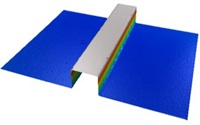
Multi-Mode Optics and ZDot™ Technology
Z-Dot Technology and True Colour Imaging
ZDot™ confocal grid structured illumination technology is the patented 3D non-contact measurement technique inside Zeta Optical Profilers. They have flexibility and upgradability enabled with multi-mode metrology, packing six powerful techniques into one compact optical package. These techniques all share a common optical path, simplifying the user experience by enabling switching between techniques without having to change the objective-sample alignment:
ZDot – Proprietary 3D measurement technology combines innovative optics with powerful algorithms to produce high resolution 3D data on a variety of surfaces and True Colour infinite focus image capture.
ZXI – Vertical Scanning Interferometry for nm-level step height accuracy over large planar areas.
ZIC – Nomarski Differential Interference contrast imaging for measuring surface roughness with sub-nm resolution.
ZSI – Shearing Interferometry using a standard objective and interference for measuring surface roughness with Å-level Z resolution.
ZFT – Film Thickness and reflectance measurement for transparent or semi-transparent materials using a broadband reflectometer.
AOI – Automated Defect Inspection using high quality camera and optics by mapping defects across the sample.
For more information on characterisation methods using Z-Dot Technology, click here.
Film Thickness Map (ZFT)Automated defect inspection and mapping (AOI) of patterned sapphire substrate.Wide area measurement of Pump Laser with high z resolution using Phase and vertical scanning interferometry (ZI)
KLA Zeta 20 Optical Profiler
Zeta-20
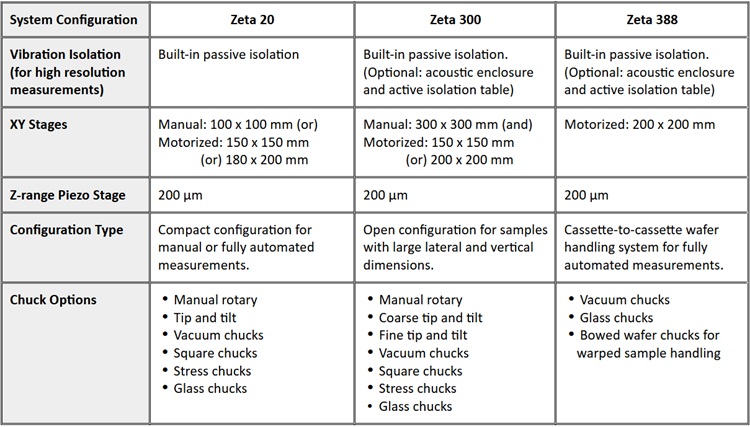
The Zeta-20 optical profiler is a non-contact, 3D surface topography benchtop system in a compact, robust package. It is powered by ZDot™ technology and multi-mode optics, enabling measurement of a variety of samples: transparent and opaque, low to high reflectance, smooth to rough texture, and step heights from sub-nanometre to millimetres. It comes with an intuitive user interface, manual or motorised XY stage and turret options, and is configurable for wafers with a diameter up to 150 mm.
The Zeta-20 supports both R&D and production environments by providing the following measurement capabilities:
Step heights from nanometres to millimetres, including high aspect ratio
Roughness of smooth (sub-nanometre) and rough (hundreds of microns) surfaces
White light interferometry for wide area step height measurements with high z-resolution.
Thin film stress and sample bow
Transparent film thickness from 30nm to 100μm with film thickness mapping.
Automated defect inspection with sensitivity for defects > 1 μm (lateral dimension).
VCSEL Device 3D surface Profile using Zeta 20
Broad Range of Applications
Photovoltaic Solar Cells: Measure surfaces with both very low and very high reflectance materials (such as low reflectance nitride and high reflectance silver paste) in the same scan using ZDot™ technology and a high measurement dynamic range.
VCSEL Device: Measure the height of the vertical cavity surface emitting laser (VCSEL) as well as actual colour of the surface using True Colour imaging, enabling visualisation of changes that cannot be observed in a 3D topography map.
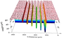
Microfluidic Devices: Measure the height, width, edge profile, and texture of channels, wells, control structures, and especially quantify changes induced by stacking layers. Laser Dicing analysis using Zeta 388 Optical Profiler
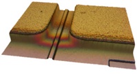
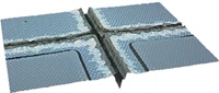
Laser Dicing: Measure the depth of a laser cut on a LED device. Measure material buildup at the edge of the cavity to determine if it has flowed outside the scribe area and into the active area of the LED device.
Biotechnology: Measure depth of deep wells and microneedle array structures for drug delivery, using the high numerical aperture objective lens and the ability to resolve a very low reflectance sample.
The Zeta-300 optical profiler is an upgrade from the Zeta-20 with integrated isolation options and configuration flexibility to support larger wafers with diameters up to 300 mm and an extended z-stage travel range up to 280 mm for very tall samples. It is also powered by ZDot™ technology and multi-mode optics and it supports both R&D and production environments by providing comprehensive step height, roughness, and film thickness measurements, plus defect inspection capabilities.
Zeta 388
The Zeta-388 builds on the capability of the Zeta-300 with the addition of a cassette-to-cassette handler and OCR and SECS/GEM support which enable measurements in a fully automated production/fabrication facility. Its configuration supports larger wafers with diameters from 100 to 200 mm.
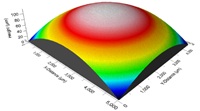
Nanometre-level Step Height Profile
Broad Range of Applications
The Zeta 300 and Zeta 388 are suitable for use in Microfluidics, Laser Dicing and VCSEL device applications mentioned above. They are also specifically useful for the following:
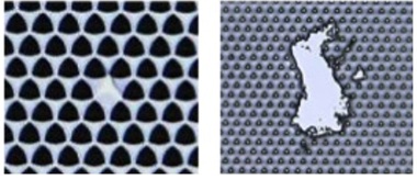
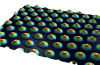
Patterned Sapphire Substrate: Measure the bump shape: height, pitch and width. Automated Optical Inspection locates defects such as contamination and missing bumps on the substrate.
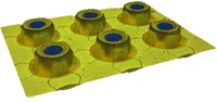
Wafer Level Packaging: Measure the height of the plated copper with the dry photoresist film intact, enabled by measuring through the transparent photoresist. Measure redistribution lines (RDL), under bump metallisation (UBM) height and texture, photoresist opening critical dimension (CD), photoresist thickness, polyimide thickness, and bump coplanarity. 3D surface Profile of Patterned Sapphire Substrate (PSS)
Nanometre Level Step Height (only with Zeta 388): Fast and precise measurements of step heights up to 250 nm with phase mode scanning (PSI), enabling tight production control of etch, CMP and deposition processes.
Zeta Solar Optical Profiler
Zeta SOLAR
The Zeta-Solar optical profiler system is the ideal metrology tool specifically designed for end-of-the-line solar process development and quality control. This new Zeta model leverages advances in 3D imaging technology to simplify the imaging system and improve the cost of ownership to the highly competitive solar cell market. It seamlessly combines easy-to-use Profilm software with the well-established solar industry-specific measurements such as metallisation finger and busbar solar process metrology. Enhanced measurement mode analysis provides solar industry-specific metallisation measurements and pass/fail output criteria. It includes XY stage options to accommodate the latest generation solar cells up to 230mm x 230mm, as well as ½ cells and earlier generation solar cells.
Hardware and Software Features
All Zeta Optical Profilers have the following hardware and software features:
Imaging: Image in brightfield, darkfield, or differential image contrast (DIC) modes. Image parameters such as field of view (FOV) and lateral resolution are determined by a combination of 5MP colour camera, coupling lenses and objectives.
Objective Lenses: ZDot™ technology eliminates the need for expensive objectives by using standard long and ultra-long working distance objectives and Mirau objectives for interferometry.
Illumination: Multiple illumination options monochromatic high brightness LED light sources to optimise performance for each application.
Fast and Easy to Use Interface: Preparing samples and equipment for data acquisition is easy with simple, intuitive software and automated measurement analysis features.
Comprehensive Analysis Suite: Automated analysis packages for each of the measurement capabilities, such as roughness, step heights, defect reviews, and so on.
Profilm3D® Optical Profilers
KLA Profilm3D Optical Profiler
The Profilm3D and Profilm3D-200 are affordable, state-of-the-art optical profilers which use white light interferometry (WLI), phase shifting interferometry (PSI) and Enhanced Roughness Mode to produce high quality 3D surface measurements, profiles and True-Colour images from the smoothest of surfaces to highly rough and steeply-sloped samples.
The newest generation of the Filmetrics ProFilm3D optical profiler is designed to enable measurements with a fine resolution on samples with larger variations in surface topography and reflectivity, and with a single tool requiring no change in setup.
They are cost-effective, easy-to-use systems suitable for measurements from polished optics to microfluidics channels , circuit boards, biological samples, biomedical devices, photovoltaic solar cells, and micro-machining. They are capable of the following measurements:
Step height
Surface roughness
Etch depth of trenches
Dimensions
Particles and grains
Volume
Bearing Ratio
Flatness
Post-wet polish of SiC surface (PSI)
They also have the following measurement modes for advanced analyses:
Phase Shift Imaging (PSI): Traditional WLI for measurement of rough surfaces suffers from low fringe contrast leading to a low signal-to-noise ratio. PSI is used when accurate measurement of nanometre scale surface features is required. The Profilm3D software easily measures defect depth, density, diameter, etc.
Enhanced Roughness Mode: This new mode increases fringe contrast, providing significantly improved fidelity on sloped surfaces and more than 70 percent signal improvement on rough surfaces, especially when the surface includes both rough topography and low reflectivity, such as some solar cells.
Total Focus™ Infinite Depth-of-Field Imaging: Unlike a traditional microscope, Profilm3D’s TotalFocus™ mode utilises the 3D measurement data to produce images where every pixel is in focus.
3D surface profile of Optical Lens created by StitchingStitching: Stitching combines multiple individual images using an intuitive software to create a larger measured field of view in applications such as MEMS, biomedical devices, curvature of optical lens (shown), etc.
Metal finishing and micromachining surface analysis using Profilm3D
Profilm3D Applications
3D and Flash Printing: The Profilm3D easily measures thickness and uniformity of the printing layer and characterises delamination, coverage uniformity and surface roughness.
Metal Finishing / Micromachining / Tooling: The Profilm3D can be used in metal finishing and tooling, such as for the critical calibration of a dicing saw where cut depths into a piezoelectric material are quantified. The system also simultaneously measures surface roughness and critical dimensions of machined components.
Semiconductors: Generates measurements of coplanarity, pitch uniformity, size, and more in applications including mask manufacturing, laser marking, photoresist patterning, etc.
Optics: For steep surfaces such as lenses, the Profilm3D in Enhanced Roughness mode can now measure up to 60°of slope.TPP thin film surface profile using Profilm3D
Biology: The Profilm3D is well suited to measurement of biological samples, such as this Tetraphenylprophyrin (TPP) thin film on glass. This image was generated with TotalFocus™ colour technology, showing the actual colours of the sample.
Contact usto discuss your specific requirements or objectives regarding optical profilers for metrology applications.