COXEM is a leading force in nanotechnology and a manufacturer of Scanning Electron Microscopes (SEM) utilising technology developed with KRISS, the Korean Research Institute for Science and Standards. With its latest products and on-going investments in research and development, COXEM Co., Ltd. is expanding the capabilities of entry to mid-level SEM analysis at affordable costs, blending cutting-edge technology with user-friendliness. It is the fastest growing supplier of Full-size and Benchtop SEM and peripheral instruments like Ion Beam Polishers and Sputter Coaters in the scientific market.
NanoTechnology Solutions is the exclusive distributor of COXEM’s instruments in Australia and New Zealand, offering installation, service and technical support for a range of applications. Contact us to discuss your Electron Microscopy needs.
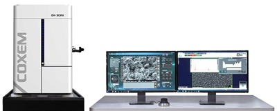
EM Series of Benchtop SEM
Benchtop Scanning Electron Microscopes (SEMs) have come a long way since their re-introduction in 2005. Gone are the days when these portable SEMs used to be limited in accelerating voltage of 15kV, resolution, selection of apertures, detectors and analytical capabilities. With growing competition in Portable SEM segment, Benchtop SEM prices from Scanning Electron Microscope suppliers have come down making electron microscopy more affordable and accessible than ever.
Previously, the luxury of multiple detector selection, better electron optics and higher analytical accuracy was only available on Full-size SEMs which not only needed significantly higher investment but was also only accessible to experienced electron microscopists.
COXEM’s EM-series product line features the most versatile Benchtop SEMs available on the market today, providing the best price/performance ratio. This series retains most of the power and capabilities of Full-size SEMs while offering ease of use for beginners in Electron Microscopy.

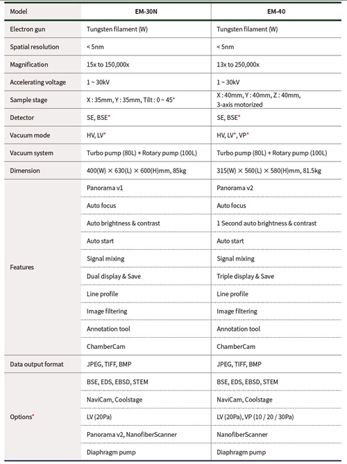
The EM-30N is a powerful Benchtop SEM designed to meet a wide range of research and quality control needs in emerging areas of nano-mechatronics. Featuring the all-new, intuitive NanoStation5 GUI, it can deliver clean and sharp high-resolution images up to a maximum magnification of 150,000x, and scan even wider areas with its Panorama Mode. It is also the world’s first Benchtop SEM that can be seamlessly integrated with a compact EDS and EBSD modules, delivering outstanding performance for rapid and high-throughput particle analysis applications. These features enable full-scale use in advanced material analyses, earlier possible only with Full-sized SEMs.
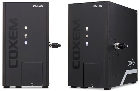
The EM-40 represents COXEM’s latest addition to their expanding family of Benchtop SEMs. The EM-40 comes with ultra-fast 5th-generation signal processing technology and provides high-quality imaging at frame rates of up to 13 fps. Compared to the EM-30N, the EM-40 system is a bit more compact with an expanded magnification range of up to 250,000x. It also has a few additional modules such as variable pressure imaging. Four imaging modes (Fast, Slow, UltraFast, and Photo) allow the user to choose the image quality and speed that best fits their application.
The EM-40PE is an upgraded system designed to scan larger samples such as membrane filters of standard size (47 × 47 mm).
Advantages and Features
» Accelerating Voltage: 1kV to 30kV
» Resolution: < 5 nm
» Magnification: 250,000x
» Auto functions: Filament, Focus, Contrast, Brightness
» Variable Pressure imaging (10, 20, 30 Pa)
» Archive Editing Function
» Nanostation GUI
» Multisample holder
» Motorised five-axis stage (X, Y, R, T, Z axis)
» Quad display / Signal mixing
» Mini Map for fine navigation
» Coloured camera navigation
» New 4 sample BF, DF STEM option!
» Panorama imaging
» 100% compatible with EBSD and EDS
» 4 Aperture sizes for best EDS and imaging
» Cooling stage option
» Unmatched detector selection
» Best in class capabilities and price/performance ratio
- Depth of Field: A high depth of field is more effective when observing an object with big undulations. To increase the depth of field, it is important to extend the Working Distance (WD) between the objective lens and specimen. The EM Series is the only Benchtop SEM that has a motorised Z axis allowing in-situ change of Working Distance. Operators can now switch between optimal Working Distance for SEM and EDS without breaking the vacuum and taking the sample out.
- High aperture range: Advanced SEMs come with moveable aperture strip with different sized apertures. Large size aperture provides greater signal for imaging and EDS work while small aperture provides very high resolution and depth of field. With EM Series, operators can move between different apertures by simply turning a knob and selecting the one delivering them the best result.
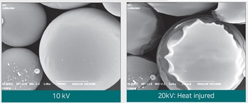
- Acceleration voltage range: Benchtop SEMs are typically limited by the maximum voltage operable. The EM Series has excellent electron optics design and 30 kV maximum accelerating voltage, delivering better than 5 nm resolution and high analytical accuracy.
The NanoStation5 GUI is the latest software interface upgraded with the following functions and new features:
- AutoFocus in 3 seconds: Auto Focus(AF) can dramatically reduce the time taken to analyse sample images.
- Fast Scanning speed: NanoStation 5.0 has greatly improved scanning speed compared to the existing EM series allowing users to select their preferred imaging speed to observe samples more quickly and clearly in various scan modes.
- Archive Editing Function: Users can re-edit the sample measurement, annotation, and other details of sample images saved in the archive.
- Location Save Function: When analysing multiple samples, users can save up to 8 preferred analysis positions and quickly observe the samples by accurately moving to the saved positions.
- Continuous MagSafe Function: Allows users to directly set various magnifications at the desired position for analysing samples, and images at the specified magnifications are automatically captured and saved.
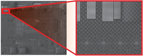
- Panorama Shot Function: Combine hundreds of thousands of SEM images side by side with its upgraded stitching function to acquire precise high-resolution images of large-area samples.
Additional Detectors and Modules
In addition to the features listed above, a range of optional detectors and modules can be installed for different application requirements. All of this while maintaining incredible ease of use!
SE/BSE Detectors
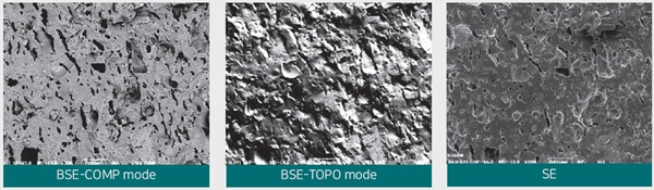
SEM allows creating images by collecting different signals. A typical example of this is information on uneven, rough surface gained by SE Detector, as well as elementary information and stereoscopic-like images gained by BSE Detector. BSE imaging is useful for gathering composition and topography features of images with high atomic number contrast.
EM-Series SEMs already feature SE detectors while the BSE detector can be optionally integrated.
Dual Display/Signal Mixing: SE + BSE Mode
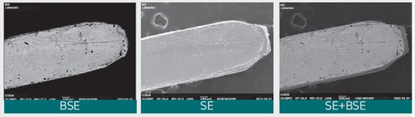
COXEM allows SE and BSE images to be obtained simultaneously in a dual display. It also offers an image merging function to combine SE and BSE images to produce images with all of their individual advantages.
Applications:
- Automotive Industries
- Material Industries
- Chemistry Industries
- Semiconductors and Electronics Industries
- Smartphones and Display Industries
Applications of STEM Detectors
COXEM offers an annular STEM detector which can be used to observe cellular tissue, nanostructures, asbestos and so on. Bright and Dark Field modes can be selected, and 4 TEM grid specimens can be loaded at once. Precise EDS analysis is possible at the same time without further adjustment.

Compact EDS-EBSD Module
The most popular option for advanced research is the simultaneous use of Electron Backscatter Diffraction (EBSD) and Energy Dispersive Spectroscopy (EDS).
Energy Dispersive X-ray Spectroscopy (EDS)
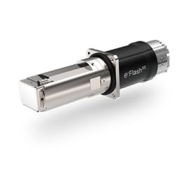
The Quantax ED-XS integrable EDS-EBSD module developed by Bruker is the most reliable and affordable package ever commercialised. It consists of the unique and revolutionary eFlash XS EBSD detector specially designed and optimised for Benchtop SEMs. Using this module, scientists are also able to perform qualitative chemical analysis such as obtaining elemental maps. The eFlash XS detector head can be easily integrated and removed to free-up the SEM chamber for non-EBSD related applications.
Multiple phases in a sample can be easily discriminated and documented based on the atomic number. The ESPRIT software suite provides fast, highly accurate quantitative and qualitative analysis of samples to determine constituent elements, including identification, concentration and distribution, useful in applications such as chemistry, automotive, construction, energy, semiconductors & electronics, metals, etc.
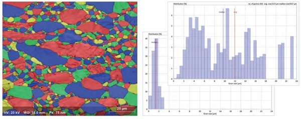
Electron Backscatter Diffraction (EBSD)
The EBSD module is useful to obtain crystallographic data of a material for applications across diverse fields such as metallurgy, materials engineering, and geology. The ESPRIT suite delivers uncompromising performance on all samples, transforming EBSD workflows. It enables grain boundary analysis, chemical and crystallographic analysis and microstructure observations to be performed with high spatial resolution. Exceptional analysis speeds on samples comprising multiple elements are balanced by extreme sensitivity, high pattern resolution and a range of innovative design features.
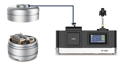
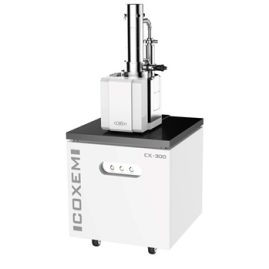
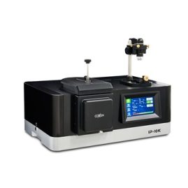
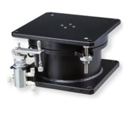
Ion Beam Polisher
Some samples may require cross-sectional polishing before SEM. Coxem’s IP-10K Ion Beam Polisher offers flat-milling, coolstage and air protection modules for the precision milling of diverse materials at the micro-scale levels, providing exceptional cleanliness and accuracy.
Air Protection Module
Samples that react rapidly and get damaged upon air exposure can be mounted within a specialised air-protection holder with a glove box filled with inert gases like nitrogen or argon. The sample can also be placed in an Ion Beam Polisher for cross-sectioning before observation in the SEM.
Low Vacuum Mode
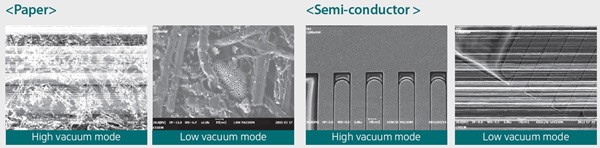
Using this mode, available as an option, you can obtain an image of non-conducting specimens such as biological samples or insulation materials which cannot be pre-treated for coating. In high vacuum, charging effect is unavoidable. By imaging the sample in low vacuum, charging effect is reduced and image is clearer. This is useful for analyses in fields such as automotive industries, material science, chemical industries, semiconductors and electronics, and bioecology.
All EM Series SEMs feature High Vacuum imaging capabilities. Low Vacuum Mode is optionally available in all of them while Variable Pressure imaging (10, 20 and 30 Pa) is available in the EM-40 system.
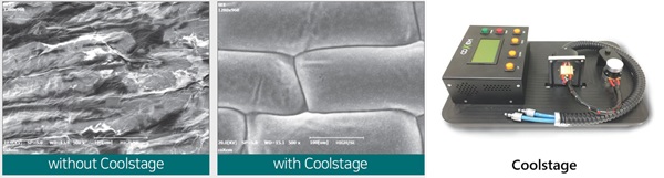
Coolstage
A biological sample requires various chemical treatments including dehydration and fixing. With Coolstage, you can observe a sample with moisture by freezing it up to 25 degrees below zero, against any damage to its structure, without a special pre-treatment.
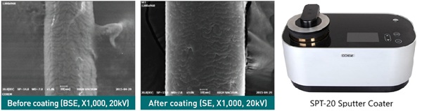
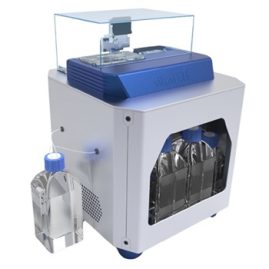
Sputter Coater
Samples that are not conductive usually need to be coated before taking SEM images. In BSE mode samples may be observed without coating. But due to charging, quality images cannot be obtained. COXEM’s versatile SPT-20 Sputter Coater provides coating of multiple metals for a range of applications.
Product Specifications