COXEM is a leading force in nanotechnology and a manufacturer of Scanning Electron Microscopes (SEM) utilising technology developed with KRISS, the Korean Research Institute for Science and Standards. With its latest products and on-going investments in research and development, COXEM Co., Ltd. is expanding the capabilities of entry to mid-level SEM analysis at affordable costs, blending cutting-edge technology with user-friendliness. It is the fastest growing supplier of Desktop and Full-Size SEM and peripheral instruments like Ion Beam Polishers and Sputter Coaters in the scientific market.

NanoTechnology Solutions is the exclusive distributor of COXEM’s instruments in Australia and New Zealand, offering installation, service and technical support for a range of applications. Contact us to discuss your Electron Microscopy needs.
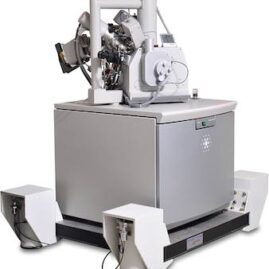
CX Series of Full-Size SEMs
The CX-200K is a standard yet robust, full-sized Scanning Electron Microscope (SEM) designed to meet a wide range of research and quality control needs. Featuring the all-new, intuitive NanoStation5 GUI, the CX-200K makes operation simple and efficient. It provides outstanding high-resolution imaging with a maximum magnification of 500,000x.
The CX-300 full-sized SEM is designed with a much larger sample stage to handle imaging of large areas of samples in imaging applications such as engine oil, geological materials, microplastics, coating paper, and so on. It provides a nano particle analysis that systematically classifies results including size, distribution, and composition of nano particles in large-area.


Advantages
» Accelerating Voltage: 1kV to 30kV
» Resolution: <3 nm
» Magnification range: 9× to 500,000×
» Motorised five-axis stage (X, Y, R, T, Z axis)
» Click & Move Stage Control
» Auto functions: Filament, Focus, Contrast, Brightness
» Detector: SE, BSE (standard), EDS (Optional)
» Chamber scope
» Unmatched detector selection
» 100% compatible with EBSD and EDS
» Variable Pressure imaging
» High Vacuum imaging
» Cooling stage option
» Multiple accessory ports available for external analytical instruments.
All COXEM SEMs share the following basic features:
- High aperture range: Comes with a moveable aperture strip with different sized apertures. Large size aperture provides greater signal for imaging and EDS work while small aperture provides very high resolution and depth of field.
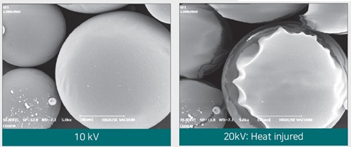
- Acceleration voltage range: The lower voltage is convenient for two occasions: when there is concern that the sample might be damaged by electron beams and when the user wishes to observe certain points of the surface.
- Depth of Field: A high depth of field is more effective when observing an object with big undulations. To increase the depth of field, it is important to extend the Working Distance (WD) between the objective lens and specimen.
SE/BSE Detectors
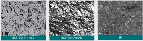
SEM allows creating images by collecting different signals. A typical example of this is information on uneven, rough surface gained by SE Detector, as well as elementary information and stereoscopic-like images gained by BSE Detector (optionally integrated). BSE imaging is useful for gathering composition and topography features of images with high atomic number contrast.
Dual Display/Signal Mixing: SE + BSE Mode
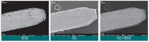
COXEM allows SE and BSE images to be obtained simultaneously in a dual display. It also offers an image merging function to combine SE and BSE images to produce images with all of their individual advantages.
Applications:
- Automotive Industries
- Material Industries
- Chemistry Industries
- Semiconductors and Electronics Industries
- Smartphones and Display Industries
Additional hardware modules
A variety of custom module options are available to modify the CX-200K and CX-300 systems for the requirements of your research and applications.
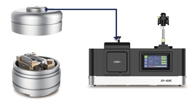
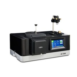
Ion Beam Polisher
Some samples may require cross-sectional polishing before SEM. Coxem’s IP-10K Ion Beam Polisher offers flat-milling, coolstage and air protection modules for the precision milling of diverse materials at the microscale levels, providing exceptional cleanliness and accuracy.
Air Protection Module
Samples that react rapidly and get damaged upon air exposure can be mounted within a specialized air-protection holder with a glove box filled with inert gases like nitrogen or argon. The sample can also be placed in an Ion Beam Polisher for cross-sectioning before observation in the SEM.
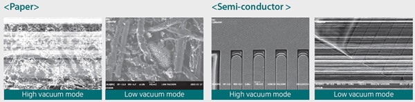
Low Vacuum Mode
Using this mode, available as an option, you can obtain an image of nonconducting specimens such as biological samples or insulation materials which cannot be pretreated for coating. In high vacuum, charging effect is unavoidable. By imaging the sample in low vacuum, charging effect is reduced and image is clearer. This is useful for analyses in fields such as automotive industries, material science, chemical industries, semiconductors and electronics, and bioecology.
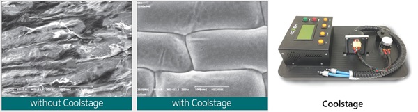
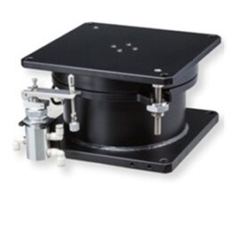
Coolstage
A biological sample requires various chemical treatments including dehydration and fixing. With Coolstage, you can observe a sample with moisture by freezing it up to 25 degrees below zero, against any damage to its structure, without a special pretreatment.
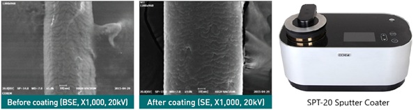
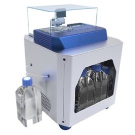
Sputter Coater
Samples that are not conductive usually need to be coated before taking SEM images. In BSE mode samples may be observed without coating. But due to charging, quality images cannot be obtained. COXEM’s versatile SPT-20 Sputter Coater provides coating of multiple metals for a range of applications.
Software Features
The NanoStation5 GUI is the latest software interface upgraded with functions and new features with such as MiniMap, Panorama Shot, Chamber Scope, Signal Mixing and etc.
- AutoFocus in 3 seconds: Auto Focus(AF) can dramatically reduce the time taken to analyze sample images.
- Fast Scanning speed: NanoStation 5.0 has greatly improved scanning speed compared to the existing EM series allowing users to select their preferred imaging speed to observe samples more quickly and clearly in various scan modes.
- Archive Editing Function: Users can re-edit the sample measurement, annotation, and other details of sample images saved in the archive.
- Location Save Function: When analyzing multiple samples, users can save up to 8 preferred analysis positions and quickly observe the samples by accurately moving to the saved positions.
- Continuous MagSafe Function: Allows users to directly set various magnifications at the desired position for analyzing samples, and images at the specified magnifications are automatically captured and saved.
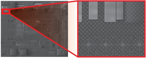
- Panorama Shot Function: Combine hundreds of thousands of SEM images side by side with its upgraded stitching function to acquire precise high-resolution images of large-area samples.

3D Reconstruction
Deep 3D, COXEM’s latest innovation, is an analysis mode that reconstructs a 3D model from a single BSE image into intuitive, revealing depth and shape of microstructures more clearly. It is pre-installed with the Nanostation5 software and is useful to study fracture surfaces, micro-defects and complex surface textures.
- One-Shot 3D imaging: No need for multiple steps. Capture a single BSE image and instantly reconstruct a 3D surface.
- Line Profile Measurement: Draw a line. Get the depth. Simply draw a line across the image to generate height profiles for precise topographic analysis.
- Texture Overlay: Bring realism into your 3D. Overlay the texture of the original SEM image onto your 3D surface to enhance visual clarity and material context.
- STL Export for CAD Integration: Seamless 3D data portability. Export 3D surfaces as STL files for use in CAD, simulation, or additive manufacturing software.
Application of STEM
COXEM offers an annular STEM detector which can be used to observe cellular tissue, nanostructures, asbestos and so on. Bright and Dark Field modes can be selected, and 4 TEM grid specimens can be loaded at once. Precise EDS analysis is possible at the same time without further adjustment.

Application of Energy Dispersive X-ray Spectroscopy (EDS)
Using COXEM’s SEM with EDS, scientists are also able to perform qualitative chemical analysis, such as obtaining elemental maps. With the BSE detector, multiple phases in a sample can be easily discriminated and documented based on the atomic number. Aztec EDS provides fast, highly accurate quantitative and qualitative analysis of samples to determine constituent elements, including identification, concentration and distribution, useful in applications such as chemistry, automotive, construction, energy, semiconductors & electronics, metals, etc.
Feature / GSR / LayerProbe

Aztec Feature combines the raw speed and sensitivity of the X-max Silicon Drift Detector with the superior analytical performance and ease of use of the Aztec EDS Analysis suite to create the most advanced automated particle analysis platform on the market.
An option for Aztec EDS microanalysis system, LayerProbe is a fast, cost-effective and high resolution thin film analysis tool with the following capabilities:
- Characterises multiple layers beneath surface of the specimen.
- Non-Destructive thin film analysis
- Lateral resolution down to 200 nm
- Easy to set-up for routine user, and a cost effective extension of SEM
Nanofiber Scanner
The Nanofiber Scanner, Coxem’s new analysis program, is ideal for analysing asbestos. It allows users to save sample images and its positions immediately at the desired location during large-area analysis.
Compatible with Contact EBSD
Coxem’s SEMs are integrated with EBSD module, useful to obtain crystallographic data of a material for applications across diverse fields such as metallurgy, materials engineering, and geology.
The Symmetry program delivers uncompromising performance on all samples, transforming EBSD workflows. Exceptional analysis speeds in excess of 3000 pps on samples comprising multiple elements are balanced by extreme sensitivity, high pattern resolution and a range of innovative design features.
Product Specifications