COXEM is a leading manufacturer of Scanning Electron Microscopes (SEM) utilising technology developed with KRISS, the Korean Research Institute for Science and Standards. With its latest products, it is expanding the capabilities of entry to mid-level SEM analysis at affordable costs. With on-going investments in research and product development, COXEM Co., Ltd. is the fastest growing supplier of SEMs and peripheral instruments like Ion Beam Polishers and Sputter Coaters in the scientific market.
NanoTechnology Solutions is the exclusive distributor of COXEM’s instruments in Australia and New Zealand, offering installation, service and technical support for a range of applications. Contact us to discuss your Electron Microscopy needs.

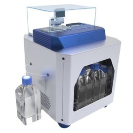
The SPT-20 is an affordable and easy-to-use digital Sputter Coater suitable for a variety of Desktop SEM and Portable Scanning Electron Microscope applications. It is used for coating the surfaces of samples with various conductive materials through the DC sputtering principle.
DC (Direct Current) Sputtering Mechanism
- In a D.C. sputter coating arrangement, the target material to be sputtered (typically conductive materials) is the cathode and the specimen to be coated is the anode.
- Upon applying a voltage between the target and the sample in a set vacuum state within the chamber, the leftover air molecules turn into plasma (ionised), and electrons and ions are formed. The ions and electrons travel at a high speed and collide with the gas molecules, and the ionisation is expedited by repelling electrons of the molecules.
- Then ion bombardment of the cathode occurs. The ensuing ions strike the cathode, resulting in the expulsion of atoms from the target material.
- Subsequently, the voltage results in one-directional deposition of the sputtered atoms on the anode where they collide and bond to form thin film coatings of the target material on the surface of the sample and work chamber.
- The deposition rate, which is affected by the pressure inside the chamber, is controlled and optimised by the rotary pump.
Why SPT-20 is ideal for SEM applications
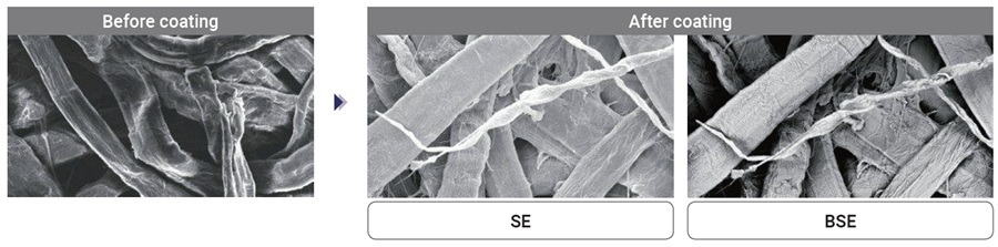
One of the main goals of Sputter Coating in SEM is to coat electrically conductive thin films on the specimens (usually non-conductive materials) to be viewed. Such films inhibit ‘charging’, protect the surfaces of sensitive samples from beam damage, and enhance secondary electron emission by increasing sample conductivity. They can even be used to form thin film-type electrodes.
The SEM requires a versatile, highly reliable sputtering system which can ensure fine grain size, uniform coating and low heat input. The SPT-20 perfectly fits these requirements with the following features:
- Multiple metallic target options such as Au, Pt, Pd, Cr, Pt-Pd, Cu, and Ni are available for sputter coating.
- It delivers stable coatings using the sputtering current feedback function.
- It makes use of a compact, low-noise rotary pump.
- The external vacuum pump (included) allows fast vacuum to be achieved and single-touch coating system up to the normal pressure. This results in adequate coated grain size for most standard SEM analyses.
- Automatic operation eliminates cumbersome process of turning the knobs and adjusting settings to a sweet spot in order to get the sputtering started.
- It has an LCD touch screen controller for easy operation.
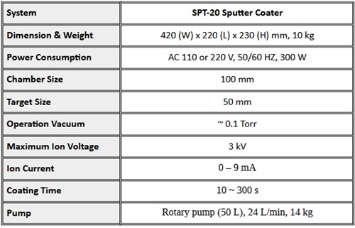
Specifications