Bruker is a manufacturer of high-performance scientific analysis instruments and advanced modules, such as the EDS-EBSD Module described here, for diagnostic solutions that empower scientific breakthroughs, research and industrial applications in a wide variety of fields.
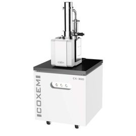
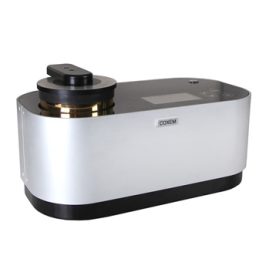
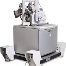
COXEM is a leading force in nanotechnology and a manufacturer of Scanning Electron Microscopes (SEM) utilising technology developed with KRISS, the Korean Research Institute for Science and Standards. With its latest products and on-going investments in research and development, COXEM Co., Ltd. is expanding the capabilities of entry to mid-level SEM analysis at affordable costs, blending cutting-edge technology with user-friendliness. It is the fastest growing supplier of Full-size and Benchtop SEMs and peripheral instruments like Ion Beam Polishers and Sputter Coaters in the scientific market. Bruker partners with COXEM to design and supply detectors and modules for multiple SEM use cases.
NanoTechnology Solutions is the authorised distributor of Bruker’s and COXEM’s instruments in Australia and New Zealand, offering installation, service and technical support for a range of applications. Contact us to discuss your Electron Microscopy needs.
What EDS and EBSD Bring to SEM Analysis
COXEM’s EM-series product line features the most versatile Benchtop SEMs available on the market today, providing the best price/performance ratio with the luxury of multiple detector selection, better electron optics and higher analytical accuracy. This series offers ease of use for beginners in Electron Microscopy, as well as quick, reliable, repeatable measurement capabilities for advanced practitioners, for general purpose imaging and quality control.
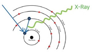
Energy Dispersive X-ray Spectroscopy (EDS) is a measurement technique that allows qualitative and quantitative elemental analysis. By collecting and detecting ‘Characteristic X-rays’ generated by deviating electrons from incident electron beams in the SEM, it is possible to identify elements, measure their concentrations, and map their distribution across a sample surface.
Electron Backscatter Diffraction (EBSD) is an analysis technique that provides crystallographic information such as spatial maps of grain structure, phase distribution, orientation, and texture. EBSD reveals microstructure, strain, and defect characteristics which are critical for geology, metallurgy, materials engineering, additive manufacturing, batteries, and energy materials.
EBSD Working Principle
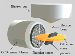
1. When a focused electron beam is directed onto the surface of a sample, a small fraction of the backscattered electrons form a diffraction pattern, called Electron BackScatter Pattern (EBSP) (or a Kikuchi pattern), on a phosphor screen placed in front of the tilted sample.
2. The energy and direction of the backscattered electrons depend on the crystallographic orientation and phase of atoms at that location, and this information is contained in the diffraction pattern. A camera inside the EBSD detector captures the pattern and transfers it to a computer for analysis.
3. The electron beam is automated to collect patterns from a grid of points across the sample surface. The camera is synchronised with the electron beam movement and can capture thousands of images/patterns per second.
4. The collected EBSPs are then analysed to determine the crystallographic orientation of each measurement point across the grid. This information is used to create a detailed spatial map of the sample’s microstructure.
Bruker’s Breakthrough: An integrable EDS-EBSD Module for Benchtop SEMs
Modern materials analysis demands both chemical identification and crystallographic characterisation. By studying the relationship between microstructural properties and macroscopic behaviour, scientists can engineer materials with specific properties that exhibit optimum performance and reliable function for their application.
EDS modules are fairly commonly available for both Benchtop and Full-Size SEMs. Until recently, EBSD detector modules were generally expensive, heavy, complex, and only compatible with large Field-Emission SEMs (FE-SEMs). Adding EDS and EBSD individual modules usually tripled the cost of an SEM system, making it accessible only to well-funded labs.
The Bruker QUANTAX ED-XS is a compact, cost-effective package that combines EDS and EBSD analyses, specifically designed to empower academic labs, teaching labs, and R&D teams to harness the power of both techniques at a fraction of the traditional cost. It offers a complete chemical + crystallographic analysis suite with semi-automated workflows for benchtop SEMs, and solves all of the above issues in path-breaking ways:
Specially designed for benchtop SEMs: The lightweight, compact EBSD detector (e-Flash XS) is optimised for small chambers and low beam currents.
True USB-3 plug-and-play module which requires no insertion mechanics.
Automatic EBSD setup and easy operation with no calibration or expert operator required.
Constitutes Field Replaceable Units (FRU) and user-replaceable phosphor screens, which dramatically lowers downtime and the costs of maintenance and ownership.
- Quick and reliable support available from local Bruker specialists
Benefits for labs with limited resources
With the above innovations, scientists and engineers in academic departments, small and medium-scale labs can now:
run routine EBSD on a benchtop system: relieve backlogs on central, expensive FE-SEMs
dramatically lower the cost of R&D and initial investment: ¼ the cost of conventional EDS–EBSD systems in FE-SEMs
train new users in EDS/EBSD safely and inexpensively
test sample preparation quality before committing time on high-end SEMs
perform combined EDS+EBSD workflows that neither technique alone can achieve
shorten cycle time for quality control with rapid compositional and crystallographic checks
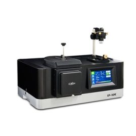
The QUANTAX ED-XS package
The QUANTAX ED-XS is a product package combining the newly developed and unique e-Flash XS EBSD detector, with the robust XFlash® 730M EDS detector under the versatile ESPRIT software suite. It is the most accessible EDS-EBSD module on the market, designed to bring full crystallographic power to benchtop SEMs.
Hardware features
EDS Xflash 730M Detector
The Xflash 730M detector provides rapid, reliable elemental analysis for all sample types on both Benchtop and Full-Size SEM systems.
30 mm² LN2-free Silicon Drift Detector
Energy resolution <129 eV at Mn Kα line
Excellent light element sensitivity
High throughput workflows such as fast mapping, line scans, point analysis
Ultra-thin window for detection of all elements ranging from boron (B) to Americium (Am).

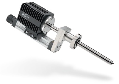
EBSD e-Flash XS Detector
The e-Flash XS is the world’s most compact, reliable and easy-to-use EBSD detector with the following features:
720 × 540 native resolution CMOS sensor
Binning modes from 2×2 up to 6×6 pixels
Camera can acquire diffraction patterns at a speed of up to 520–525 frames/second even at moderate electron probe currents.
User-removable detector head (slide-in/out)
User-replaceable phosphor screen
USB3 plug-and-play for power and data transfer with PC
Optical system designed for maximum light transmission to detector
Integrated Software Suite (ESPRIT)
The high-performance ESPRIT software completes the package to create a powerful, yet easy-to-use analytical tool. Chemical and crystallographic data are acquired, processed, and evaluated using the same software, thus enabling the following features:
Automatic pattern centre adjustment: no calibration required
Automatic gain optimisation and control
Automatic crystal phase setup
Real-time indexing
Up to 60,000 points/s reindexing speed
EDS spectra quantification at up to 2,000 spectra/s
Grain reconstruction: CSL boundaries, shape & size distributions
Phase differentiation combining EDS + EBSD
Orientation maps, texture, inverse pole figure plots
Quick setup for routine EBSD jobs
The ESPRIT suite offers outstanding advantages in the seamless integration and combined processing of datasets. To minimise the SEM usage time required to setup the EBSD measurement on samples with unknown type and number of phases, one can launch the acquisition of an EBSD Map and an EDS HyperMap without identifying all phases immediately. The EDS HyperMap shows the spatial distribution of element containing one EDS spectrum for each of its ~300,000 pixels and is acquired simultaneously with the EBSD map at a speed of upto 100 points/second. The phase identification can be done offline at a later time using the ultra-fast re-indexing power of the ESPIRIT Software.
Installation & Operational Benefits
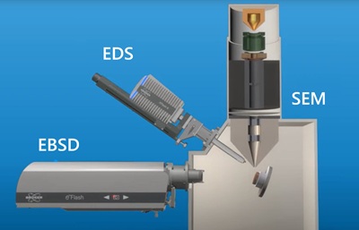
Coxem’s EM-30 and EM-40 systems are the world’s first Benchtop SEMs that can be seamlessly integrated with a compact EDS-EBSD module. Benchtop systems typically have only one chamber port used for the EDS detector. Coxem’s systems are the only series on the market with multiple chamber ports (three), and the Quantax ED-XS is designed for mounting the X-flash and e-flash XS detectors on these ports. The detector heads can be easily removed to free up the chamber for general SEM imaging.
It is also perfect for checking sample preparation for EBSD before using a high-end FE-SEM making it easy for new users and ideal for teaching labs. The result is the most accessible EBSD platform ever introduced for small laboratories, universities, and industrial R&D.
Why EDS+EBSD Together Is More Powerful
EDS and EBSD are two techniques that provide very different measurements, and there are certain types of analysis EDS alone cannot do and vice versa. When you have an integrated system it expands the research for specific applications where the two techniques complement each other. The following are examples where a specific challenge is solved by combined EDS-EBSD analysis:
Chemically identical but crystallographically different materials: Titanium oxide has two well-known polymorphs – anatase and rutile TiO₂. The two crystal phases can only be distinguished by EBSD (analysis shown in figure above).
Crystallographically similar but chemically distinct materials: Metals such as Cu, Ni, Au, Ag, have very similar Kikuchi patterns. Here, EDS is used to differentiate the elements in a spatial map.
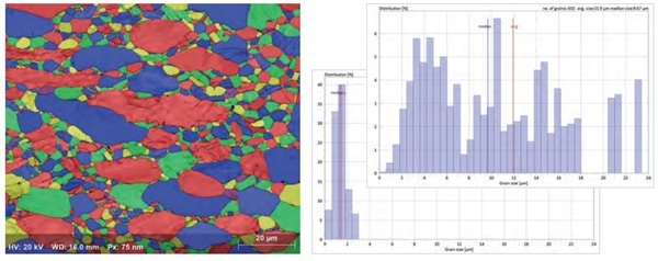
Grain size / grain shape / texture of surfaces: EBSD provides fully automated analysis of the orientation, size and shape distribution of grains in crystalline materials. This provides insights into preferred orientations of grains, which is crucial for predicting and engineering material or device properties.
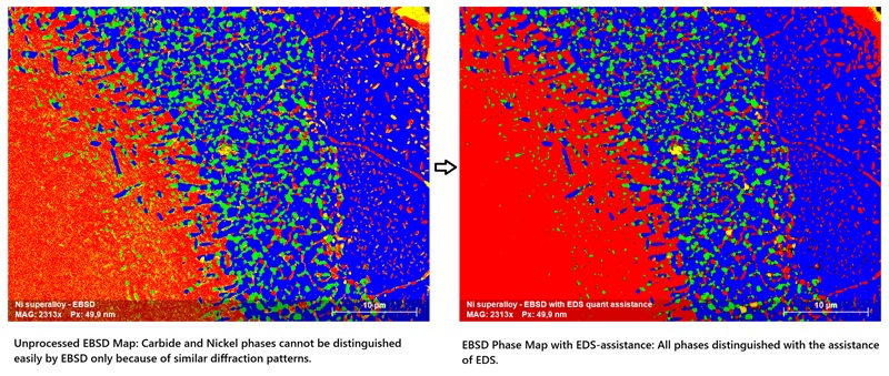
Phase distribution: In this study (below) of a characterisation of a thermal barrier coating on Ni Superalloy, the challenge was to successfully distinguish the carbide from the nickel matrix phase. Both have cubic fcc structure and therefore produce very similar diffraction patterns. To this aim, the map was corrected offline by EDS assisted EBSD indexing.
For more information on possible applications and analysis methods, click the links below:
- Correlation of Grain Statistics with various Properties on Industrial Alloys
- Phase Determination & Grain Size Analysis of Duplex Steel
- Characterisation of Microstructural Features in Stainless Steels
- Correlation of Grain Statistics with various Properties on Industrial Alloys
- Phase Identification and Distribution Analysis of Little-known, Multi-phase Containing Materials
- Phase Identification & Distribution Analysis of Oxide Ceramics
Applications of the EDS-EBSD Module Across Industries
The Quantax ED-XS module finds applications in a wide range of fields where rapid EDS-EBSD analyses using benchtop SEMs is in demand:
Materials Science & Metallurgy
Grain size, shape, texture and orientation analysis
Recrystallisation and phase transformation analysis
Orientation and phase maps
Energy & Battery Materials
Crystallography of cathode/anode materials
Solid electrolyte interfaces
Texture in deformed metal sheets and foils
Lithium metal dendrite orientation studies
Semiconductors & Electronics
Thin film characterisation
Interconnect grain orientation
Device failure analysis
Manufacturing and Quality Control
Coating analysis
Lightweight alloy analysis
Metallographic inspection
Heat treatment evaluation
- Failure analysis, lifetime prediction assessments
Geology & Mineralogy
Mineral phase identification
Large-area EBSD mapping
Mineral texture & composition analysis
Biology & Biomedical Engineering
Structural analysis of biominerals, implants
Forensics
Gunshot residue (GSR) detection and analysis
Microstructural signature matching
How to make decisions regarding SEMs and EDS, EBSD Modules?
For low budgets / low-risk investments: EM-30 with ED-XS provides integrated EDS and EBSD capabilities for ~1/4 of the cost of a conventional solution.
For larger budgets: 4x EM-30 with ED-XS. It is a similar investment as for a conventional system but the lab will have almost twice the productivity and still be at 75% capacity if one system fails (SEM, EDS, or EBSD components)
Explore specifications, request a demo, or contact our team to learn how to integrate the EDS-EBSD module into your benchtop SEM.