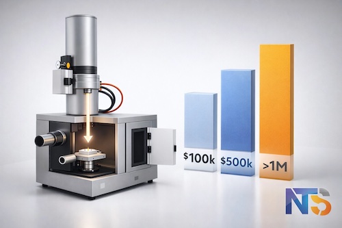
Purchasing a Scanning Electron Microscope represents one of the most significant capital investments a research facility or industrial laboratory will make. The scanning electron microscope price spectrum ranges dramatically: from approximately $90,000 for entry-level benchtop systems to well over $1 million for high-end field emission instruments with advanced analytical capabilities.
Understanding what drives these cost variations allows procurement teams, facility directors and laboratory managers to make informed decisions that align instrument capabilities with actual research requirements. The electron microscope price reflects far more than the imaging system itself: it encompasses resolution specifications, detector configurations, automation features, ongoing operational expenses, and installation infrastructure, including vibration isolation where required by site conditions.
Factor 1: Resolution and Magnification Capabilities
The resolution specification serves as the primary cost determinant in SEM pricing. This parameter directly correlates with the sophistication of the electron optical column and the type of electron gun employed.
Entry-level tungsten filament SEMs typically achieve resolutions between 3-10 nm at optimal working distances. These systems provide adequate performance for routine industrial quality control, failure analysis, and educational applications. Magnification capabilities generally reach 100,000x to 300,000x, sufficient for most materials characterisation tasks.
Field Emission Scanning Electron Microscopes (FE-SEM) deliver substantially higher performance, achieving resolutions below 1 nm with magnification capabilities extending to 1,000,000x or higher. This performance comes from the fundamentally different electron source technology and more sophisticated lens designs required to maintain beam coherence at extreme magnifications.
The cost differential between these categories can exceed $300,000 to $900,000. Laboratories conducting nanomaterials research, semiconductor inspection, or advanced biological imaging at the cellular organelle level require FE-SEM capabilities. Facilities focused on micron-scale surface analysis or metallurgical examination often find entry-level systems more cost-effective.
Consider actual magnification requirements carefully. Many applications rarely exceed 20,000x magnification, making ultra-high resolution capabilities an unnecessary expense. Define the minimum resolvable feature size critical to your research before committing to high-end specifications.
Factor 2: Detector Configuration and Analytical Capabilities
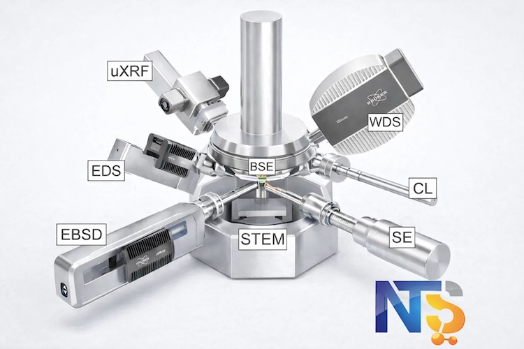
The detectors package substantially influences the cost of electron microscope systems. Each analytical capability requires dedicated hardware that adds both purchase price and system complexity.
Standard secondary electron detectors provide topographical imaging and come included with virtually all SEM systems. Beyond this baseline, each additional detector represents a significant cost increment:
Backscattered Electron Detectors (BSE) enable compositional contrast imaging and add approximately $15,000 to $30,000 depending on configuration. These detectors prove essential for materials science applications where atomic number contrast reveals phase distributions or compositional variations.
Energy Dispersive X-ray Spectroscopy (EDS) systems provide elemental identification and quantitative composition analysis. Complete EDS packages range from $40,000 to $100,000 depending on detector size, resolution, and software capabilities. Multi-user facilities conducting diverse materials characterisation consider EDS nearly essential, while specialised applications may not require this capability.
Electron Back-Scatter Diffraction (EBSD) detectors enable crystallographic orientation mapping and phase identification. These sophisticated systems add $80,000 to $150,000 to instrument costs but provide unparalleled insights into microstructure, texture, and grain boundary characteristics critical for advanced materials development.
Cathodoluminescence detectors (CL), Wavelength Dispersive Spectrometers (WDS), and specialised in-situ capabilities represent additional options that address specific analytical requirements at corresponding cost increases.
The strategic approach involves identifying which analytical techniques your research actually requires versus capabilities that might occasionally prove useful. Each unused detector represents capital tied up in under-utilised functionality.
Factor 3: Automation and Software Sophistication
Automation capabilities significantly impact both purchase price and long-term operational efficiency, particularly in multi-user facilities or high-throughput environments.
Basic SEM systems require manual optimisation of imaging parameters: focus, astigmatism correction, brightness, and contrast adjustments. Experienced operators achieve excellent results, but the learning curve limits accessibility for occasional users. Entry-level systems generally include fundamental imaging software with limited automated features.
Advanced automation packages incorporate automatic focus and stigmation correction, intelligent beam current optimisation, and guided workflows that reduce operator intervention. These features substantially improve accessibility in university core facilities where users possess varying expertise levels.
Automated stage control and large-area montaging capabilities enable unattended imaging of entire sample surfaces or systematic survey of multiple specimens. This functionality proves particularly valuable in semiconductor inspection, forensics applications, and quality control environments requiring statistical sampling across many features.
Image analysis and quantification software ranges from basic measurement tools to sophisticated packages incorporating machine learning algorithms for automated feature recognition and classification. Advanced software suites can add $20,000 to $80,000 to system costs but dramatically enhance productivity in routine analytical workflows.
Consider the actual user base and throughput requirements. Laboratories supporting occasional specialised imaging by expert operators may not justify expensive automation. Multi-user core facilities serving diverse research groups often find automation packages provide excellent return on investment through improved accessibility and reduced training requirements.
Factor 4: Maintenance and Operating Costs
The scanning electron microscope price encompasses far more than the initial capital outlay. Ongoing operational expenses accumulate substantially over a typical 10-15 year instrument lifetime.
Electron source replacement represents the most predictable recurring expense. Tungsten filaments cost approximately $50-150 each and require replacement every 40-100 hours of operation. Lanthanum Hexaboride (LaB6) and Cerium Hexaboride (CeB6) cathodes cost $800-2,000 but last 1,000-2,000 hours. Schottky field emission sources range from $5,000-15,000 with lifespans exceeding 2,000-5,000 hours under proper operation. The LaB6, CeB6 and FE sources require a service engineer to conduct the source replacements which can add several thousand dollars to the annual operating cost while the Tungsten filaments can be easily and quickly replaced by the SEM users.
Service contracts typically cost 8-12% of system purchase price annually. A $300,000 SEM might incur $24,000-36,000 yearly service expenses. These contracts cover preventive maintenance, vacuum pump overhauls, and priority response for component failures. Self-maintained systems reduce these costs but require trained personnel and parts inventory.
Consumables and utilities add additional operational expenses. Vacuum pump oil, roughing pump maintenance, and occasional vacuum system refurbishment accumulate over time. Calculate total cost of ownership over the expected operational lifetime. A less expensive system with high maintenance costs may prove more expensive long-term than a higher-priced instrument with reduced operational expenses.
Factor 5: Specialised Requirements and Custom Capabilities
Application-specific requirements often drive significant cost increases beyond standard SEM configurations.
Large specimen chambers accommodate bulky samples that exceed standard stage dimensions. Semiconductor wafer inspection, forensic evidence analysis, and paleontological specimens may require chambers accepting 200-300 mm samples. These configurations add $40,000-100,000 depending on chamber size and motorized stage requirements.
Cryo-SEM capabilities enable imaging of frozen hydrated samples critical for biological ultrastructure research. Complete cryo-transfer systems with temperature-controlled stages add $80,000-150,000 but prove essential for specific life science applications.
Variable pressure or environmental SEM (ESEM) modes allow imaging of non-conductive or outgassing samples without conductive coating. This capability requires specialised differential pumping systems and detectors that increase system costs by $50,000-120,000.
In-situ analytical capabilities like heating/cooling stages, tensile testing stages, nanoindenters enable dynamic experiments within the SEM chamber. These specialised accessories range from $25,000 for basic heating stages to over $200,000 for sophisticated mechanical testing systems.
Evaluate whether specialised capabilities justify their substantial costs or whether sample preparation alternatives might achieve similar outcomes more economically. For surface cleaning before SEM imaging, use plasma cleaning and the O₂ vs H₂ vs Ar: The Proven Plasma Cleaning Gas Selection Framework to match gas chemistry to contamination type and substrate constraints.
Making Informed SEM Investment Decisions
Comparing scanning electron microscope prices requires understanding the specific factors driving cost variations and assessing which capabilities your research programs require versus features that may remain under-utilised.
NanoTechnology Solutions provides expertise in SEM detector systems, accessories, and analytical upgrades that optimise instrument performance for specific applications. Multi-modal laboratories also commonly pair an Atomic Force Microscope and AFM workflow with SEM for correlative surface characterisation, which can influence how capital budgets are allocated across imaging platforms.
The most cost-effective SEM investment matches instrument specifications precisely to research requirements without paying for unnecessary capabilities or sacrificing critical performance parameters.