The KLA Instruments comprehensive portfolio of products, software, analysis, services and expertise is designed to help scientists, researchers and engineers address their toughest measurement challenges in the characterisation of diverse samples by generating reliable, precise data. Through use of these products and services, they are better able to deliver the breakthroughs that impact their respective fields.
NanoTechnology Solutions is the exclusive distributor of KLA Instruments and supplies, installs, supports surface metrology products and accessories across Australia and New Zealand.
Contact us to discuss your specific requirements or objectives regarding metrology with our Optical profilers.

Surface profilometry is an essential metrology tool that is used in a wide variety of applications, such as semiconductor packaging, HBLEDs, glass manufacturing, solar cell fabrication, hard disk manufacturing, and many others. Optical metrology has the advantage of providing uniform lateral resolution without contacting potentially delicate surface features.
Apart from the phenomenal advantage in speed of acquisition over old-fashioned stylus-profilers (a competent 3D Optical Profiler, for instance, typically acquires a full 3D map in about 30 seconds and is fast and easy to set up for each run) there is a host of other serious benefits, such as true colour mapping and the ability to cover height measurement ranges from sub-nanometre to millimetres (neither of which can be done with interferometers) and to take extremely bulky samples in situ.
As compared to a conventional microscope, the non-contact Zeta optical profiling, combined with Å-level step height accuracy, provide an infinite depth of focus, producing 3-dimensional images with all surfaces clearly displayed in sharp focus. This capability is especially important for handling structures with large Z variation, such as MEMS devices, micro lenses, and semiconductor packaging structures across a wide range of applications such as solar cells, semiconductor and compound semiconductor devices, biological applications, and more.
This is made possible with KLA’s proprietary ZDot Technology developed in-house to support the breadth and depth of these measurement modalities. The Zeta™ optical profilers are also available with enhanced differential interference contrast imaging (ZIC), shearing interferometry (ZSI), vertical scanning interferometry (ZXI), and reflectometry (ZFT).
ZDot Technology

At the core of Zeta optical technology is the KLA-proprietary ZDot measurement technique, with a structured illumination that uses confocal optics. A grid is projected onto the surface at the focal plane, which can be thought of as an array of pinholes. There is no need to raster in XY, but scan only in Z to determine the signal from each grid point, which is maximised. As the optics move in the Z direction, the projected grid comes into focus at different points along the sample surface height, which provides Z mapping data in the field of view.

This innovation provides the following benefits:
- This method generates local contrast on surfaces where no native sample contrast exists. This enables the most featureless, smooth, and polished surfaces to be 3D-mapped unambiguously.
- The Z-Dot technology includes unique transmissive and dark field illumination methods that enable the Zeta profilers to handle the most challenging applications, such as high roughness surfaces, very dark surfaces, deep trenches, and multi-layer transparent surfaces.
- The precise scanning in the Z direction is based on signal contrast analysis, which eliminates the signal intensity limitation of traditional confocal techniques.
- ZDot technology is further enhanced through the integration of other functionalities such as:
- Vertical scanning interferometry (ZXI) – for nm-level step height accuracy over large planar area
- Nomarski Differential Interference Contrast imaging (ZIC) – for measuring surface roughness with Å-level Z resolution
- Shearing interferometry (ZSI) – for measuring surface roughness with Å-level Z resolution
- Film thickness measurement (ZFT) – for transparent or semi-transparent materials using a broadband reflectometer.

Z-Dot measurement mode simultaneously collects a high-resolution 3D scan and a True Colour infinite focus image of a VCSEL device. Source: KLA Instrument - ZDot Film – measures through transparent films to calculate thickness for photoresist, polyimide, and even highly non-uniform films, such as spin-coated photoresist near the edge of a wafer.
- These techniques all share a common optical path, simplifying the user experience by enabling switching between techniques without having to change the objective-sample alignment.
For example, in a conventional optical profilometer with a 100X objective, the vertical resolution is ~ 0.7μm. However, using ZDot™ mode, the vertical resolution of the 100X objective is improved to 0.013μm using the confocal Zdot™ grid.
Another example of a measurement which is enabled by the use of Zdots™ is the ability to measure micro needles (see for instance the paper on 3D maps of micro needle arrays by Prof. Y. Makino et al).
3D surface roughness characterisation
Zeta optical imaging can also measure surface texture roughness. The Zeta-20 was used to measure the surface topography and roughness of the inner filtration layer of a N95 face mask. Measurements were taken prior to and after disinfection treatment by UV exposure. Fiber width comparison data verified the narrowing of the fibers following UV exposure.
Surface Roughness of Sapphire wafers

RMS Roughness of 1.41 um, measured by a P-17 Stylus Profiler (left). RMS Roughness of 1.39 um, measured by a Zeta-20 Optical Profiler (right). Source: KLA Instruments
Surface roughness can be quantified using an optical profiler such as the Zeta-20. Traditionally, sapphire wafer manufacturers measure roughness using a 2D scan from a stylus profiler, such as a Tencor™ P-17 Stylus Profiler. For this comparison, the P-17 was configured with a 2μm radius stylus, which has a resolution of about 1μm in XY, and 1nm in Z. Although 2D profiles can be used as the basis for RMS roughness measurement, it is important to maintain sufficient sampling so that the measured roughness is representative of the surface as a whole.
A single 2D scan takes about 10 seconds, whereas the high-resolution 3D scan takes over 10 minutes to acquire but provides much higher sampling. 3D scans can be quickly generated by the Zeta-20 optical profiler. For a typical XY resolution of approximately 1μm, the full field of view can be imaged in seconds with high-resolution 3D sampling, providing additional information to enable better process control.
In comparing the stylus profiler data to the optical profiler data, although the 3D roughness results are very similar, the Zeta-20 quickly provides the 3D area data in about the same time it takes to acquire a single 2D scan on the stylus profiler.
Although RMS roughness can be used as a starting point for roughness measurement, higher-order surface roughness parameters such as skew measurements and Abbott curves can be used to provide more in-depth surface texture analysis for surfaces such as porous chucks.
Deep Trench Characterisation

The demand for accurate characterisation of high aspect ratio geometries such as narrow gaps, deep trenches or deep holes arises in many technologies and industries.
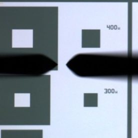
When measuring deep trenches, it is challenging for some types of profilers to measure high aspect ratio structures, especially for features with narrow openings. For example, a stylus profiler generally works best for samples with aspect ratio < 1:1, due in part to the included angle of the stylus tip. White Light Interferometry (WLI) is favourable for its excellent z resolution, but the performance may be unsatisfactory for samples with high surface roughness.
Among the candidates for this type of metrology, 3D optical profiling characterisation is adopted widely due to its non-destructive measurement method and excellent data accuracy, especially advantageous for delicate samples.
It is also possible to perform additional topographical analyses with the same instruments. Full characterisation of a deep trench is important, because the surface roughness and shape of the trench edge have a large influence on device performance.
The Zeta-20 system utilises the proprietary ZDot™ measurement technique to non-destructively characterise deep trenches with varying width and aspect ratio. They can measure deep trenches with widths ranging from 10μm to 200μm and even larger.


The roughness of the etched silicon surface is another key parameter for further process development. The unique feature detection function of the Zeta tools enables automatic detection of areas of interest within the field of view (FOV) and can also measure the bottom roughness of all trenches collectively. Because this measurement method is automated, the Zeta software is ideally suited to characterise arrays of trenches to provide measurement statistics for the whole wafer or for multiple wafers measured in production mode.
Contact us to discuss your specific requirements or objectives regarding metrology with our Optical profilers.